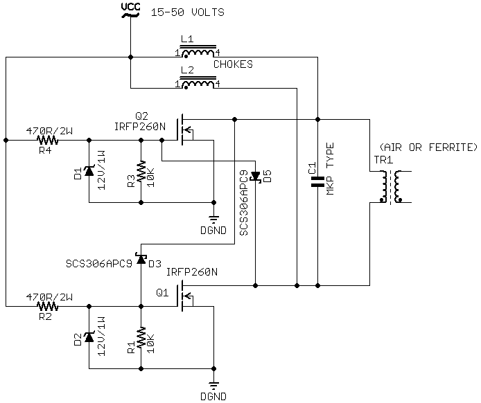
Schematic 1. Basic ZVS Driver
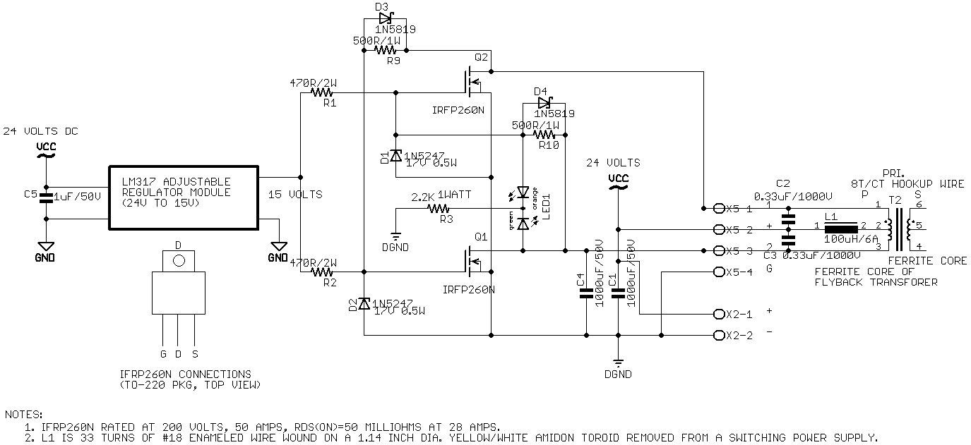
Schematic 2. ZVS Driver with CT Primary
Page 2
This note describes the operation of a "ZVS" (Zero Voltage Switching) driver used in a number of YouTu be demonstrations for high voltage flyback and induction heating drivers. This note is the result of research I did on this circuit when investigating induction heating.
This circuit was introduced by Vladimiro Mozilli around 2009 and is often called the "Mazilli" driver. Although there are excellent tutorials and demonstrations on this driver on YouTube, the purpose of this note is to explain the basic operation of the ZVS circuit and to offer recommendations for its construction, operation and use.
The circuit initially was used as a high voltage driver for CRT flyback coils. Later, the same circuit was employed to drive induction heating coils.
This video shows tests on a 1000 Watt induction heater board.
This EBay listing shows a typical 1000 Watt induction heater.
Here is an interesting site that discusses the driver when used as a flyback driver. This same site also discusses the driver when used for a ZVS induction heater.
Page 3
Page 4
Page 5
The ZVS Driver circuit is a Royer-type push-pull oscillator with a resonated primary that is implemented with FETs. This type of oscillator can be used to drive the ferrite core of a flyback transformer to generate high voltage. It can also drive a high-current air-core "work" coil for an induction heater.
The high voltage driver was originally touted as an improved way of driving flyback cores. Until the introduction of Mazilli's circuit, flybacks were typically driven with a single transistor and a feedback winding or with a push-pull transistor configuration (e.g., using two 2N3055 transistors).
The operation of the circuit is descibed below, including its drawbacks and improvements. The operation also discusses selection of components, an area that is typically not well-covered at most sites.
It appears that component selection is not well understood because of the unique characteristics of a resonant Royer-type oscillator. The component stresses are considerable with this type of circuit because of the resonant operation of the primary which generates large voltages and currents that can stress poorly-selected components.
Page 6
This section describes the basic operation of the ZVS Driver, including the design and purpose and selection of components. The descriptions below refer to Schematic 1 and Schematic 2.
The ignoring the power supply chokes and resonating capacitor(s), the ZVS circuit is simply a push-pull FET-based oscillator where the drain of each FET is cross-coupled to the gate of the opposite (out of phase) FET.
The operation of this kind of driver for the primary of a transformer is very straightforward and need not be discussed here.
The circuit is fed from the power supply through a center-tapped primary coil and a single choke or from two separate chokes connected to the FET drains (as shown in Schematic 1).
With the two (47uH-200 uH) choke coils and the resonating capacitance across the primary, the circuit operates as a "Royer" type inverter where the primary is resonated with the capacitance and where the chokes keep the power supply from reducing the resonant action of the primary. These chokes also keep the primary oscillations from feeding back to the power supply. The role of these chokes and the resonating capacitor are discussed more fully below.
Zener diodes are connected across the FET gates so that the maximum gate to drain voltage is not exceeded. Use of a zener voltage higher than the minimum gate to source turn-on voltage ensures that the FETs are conducting at a high level.
Page 7
The "fast diodes" connecting the drains to the opposite side FET's gate are typically Schottky diodes or fast recovery diods (FREDs). These diodes provide a fast turn off of the FET gates when they are driven toward ground as the opposite-phase FET saturates. Although the forward-biased diode of zener can be used, it is significantly slower than the Schottky diode.
Each FET is turned off as the opposite-phase FET turns on and this continues until the primary voltage reverses phase. This phase reversal happens when the primary voltage crosses zero so that switching occurs when there is zero voltage across the FET. Hence, "Zero Voltage Switching" or ZVS.
In some cases, the FETs are run without zeners to ground and the gate voltage is limited by a voltage regulator such as a 7812. With this configuration, the resistors from the power supply to the gate can be lower (e.g., 270 Ohms), thus reducing turn on time. Note that the gate bias voltage must be lower than the drain supply voltage to ensure that the coupling diodes are reverse biased when the drain is high. Also note that the dissipation of the gate bias resistors should be carefully watched as their resistances are reduced.
Page 8
Because of the resonant voltage rise in the primary, the FET drains must withstand more than 2 times the power supply voltage. Most designs recommend a voltage rating of 3 to 4 times the supply voltage.
For a supply voltage of 24 Volt, the FETs should be rated conservatively at 200 Volts or higher.
Because of the resonant current rise in the primary, the FETs must be able to handle currents about 4 times the nominal power supply current. This requirement is normally satisfied by selecting FETs that have high continuous drain currents and Rds(on) resistances of less than a tenth of an Ohm.
A typical FET recommended for several designs is an IRFP260N rated at a voltage of 200 Volts and a drain current of 50 Amps. Drain "on" resistance is 0.04 Ohms and power dissipation is 300 Watts. The cost at Mouser is under $3.00 in small quantity. Here is the IRFP260N datasheet
Another consideration for the FETs is the gate to source capacitance (gate charge), which should be minimized to improve FET turn-on and minimize FET dissipation. With reasonably fast switching, dissipation requirements can normally be satisfied with relatively small heat sinks (e.g., because of fast switching and ZVS operation). A small heat sink or on-board copper fill can generally provide the needed dissipation of a Watt or so.
Page 9
As noted earlier, the zener diodes limit the FET gate to source voltage to the maximum specified in the spec sheet. A 15 Volt zener, rated at at least one Watt, is commonly used in most ZVS circuits. The zener limiting resistors not only limit the maximum dissipation of the zeners but also drive the gate to source capacitance of the FETs. A separate regulated gate supply voltage, should be set less than the zener voltage and the nominal FET drain voltage. Or, the zener can be eliminated or substituted with a reverse-biased diode. If the gate supply voltage is at the same voltage as the supply voltage, the zener dissipation should be checked for the operating voltage.
For fast operation, the zener current limiting resistors should be as small as possible while not challenging any power ratings.
The resistors are typically tied to the power supply which can cause both zener and limiting resistor dissipation problems when increasing the supply voltage. As previously noted, a better design is to use a separate gate power supply fed off the main power supply, as shown in Schematic 2.
Because the driver I built operates at 24 VDC, the gate bias voltage was established by regulating the 24 Volt supply down to 15 Volts with a small LM317 regulator board. The board's trimpot was adjusted for an output of 15 Volts. Using this approach, the bias supply can be regulated with only the requirement that the power supply voltage is always at least a few Volts larger than the desired output voltage (15 Volts). See Schematic 2 for the regulator connections.
Page 10
The cross-coupling diodes should be Schottky types with a voltage rating consistent with the power supply voltage and resonant rise considerations. Diodes rated at more than 200 Volts are commonly-available and can be "pulls" from old switching power supplies.
Some designs use the popular 1N5819 Shottky diode but its rating is only 40 Volts (use something else). One diode I found on a quick part search is a SCS306APC9. It is available from both Digikey and Mouser for under $3 (qty 10). It is rated at 650 Volts and 6 Amperes (available in a TO220 package).
Another fast diode in a TO220 package would be a FFPF30UA60S rated at 600 Volts and 30 Amperes. It is available from Mouser for about one dollar (qty 10).
Page 11
The sample circuit diagram shows two chokes connected between the power supply and each leg of the primary. Some circuits use center-tapped primary and a single choke between the center tap and the power supply. In some designs a single ferrite core with two windings is used in a common-mode filter configuration. This saves a core but still allows a separate feed to each FET drain and eliminates the center-tapped.
There seems to be some confusion about the chokes and their ratings. The impedance of the choke must be somewhat higher than the impedance of the primary but must also be able to handle the current drawn from the power supply and power losses in the core.
Typically, the choke is wound on a powdered iron (Material 26). With this material's relatively low permeability (75), the core will not saturate at the maximum power supply current. Saturation is generally not a concern unless a toroid with an extremely high permeability is used (e.g., values greater than 200). A typical choke value for a ZVS driver operating near 100 kHz is around 100 microhenries.
The wire used in the choke must be able to handle the maximum current demanded of the power supply without significant core losses.
Some reported bad results are probably due to poor construction of these chokes. It is probably not a good practice to use randomly-selected toroids removed from old switchers without first testing their performance, especially with rated load current in the winding. It is probably best to separately test the chokes before deploying them or to incorporate them in a final design and board layout.
Page 12
Chokes salvaged from junk switching supplies can be a good source of pre-wound chokes or bare cores, provided that they are tested at their frequency of use. Using "yellow core" powdered iron toroids may require over 30 turns to get the appropriate inductance (around 100 uH for circuit shown in Schematic 2).
Using a relatively high number of turns increases the current rating of the choke (assuming the "NI" factor in Faraday's law. The DC resistance of the wire should be low enough for the desired average drain current without overheating. The FET drain's resistance should also be much smaller than the DC resistance of the choke wire (say 130 milliohms). The IRP260 FETs shown in Schematic 2 have a drain resistance of 40 milliohms at a drain curent of 28 Amperes.
In one home-brew ZVS design, the chokes each consisted of 14 turns of hookup wire wound on a ferrite transformer removed from a switching power supply. The inductance was approximately 130 uH.
I removed and measured the single center-tap choke for the commercial flyback driver. The core was yellow with 33 turns of #18 enameled wire and an inductance of 103 uH.
A yellow/white painted toroid core of about the same size (25 mm outside diameter) was removed from an old switching power supply and was tested with the same number of turns of #18: its inductance value closely matched that of the commercial core. Substituting the home-brew choke for the commercial choke did not appear to change the operation of the flyback driver.
From an Amidon manual, the powdered iron core material is probably type 26 with a permeability of around 75. This material is specifically designed for low-Q choke or line filter applications. According to Amidon's color coding, the core is painted yellow and white, just like the toroid salvaged from the power supply.
Page 13
The impedance of the 103 microhenry commercial choke at the operational frequency of 77 kHz is 49.8 Ohms. The operational frequency was measured with the flyback secondary producing a continuous arc, as shown in Photo 2" Note that photos of waveforms with a frequency above 70 kHz indicate that the output is drawing a continuous arc.
Without an arc (transformer secondary left open), the operational frequency is approximately 38.3 kHZ. At this lower frequency, the 103 uH reactance is approximately 11.1 Ohms.
The inductance of the primary of the ZVS driver is 22.8 uH with a reactance of 12.9 Ohms at 77 kHz. Thus, the ratio of the choke impedance to the primary impedance (with a sustained arc) is approximately 4 to 1 (49.8/12.9).
The above indicates that, ideally, type 26 material can be used as a ZVS driver at a power level of approximately 200 Watts. If a surplus core cannot be salvaged from an old power supply, the choke toroid can be ordered from Amidon.
Rewinding the "junk" 25 mm yellow/white toroid using 15 bifilar turns of #18 enameled wire and connecting the windings in a series-aiding configuration yields an inductance of 91.8 microhenries, thus validating the previous winding results. This bifilar winding technique reduces the trauma of winding a large number of turns on a toroid core.
Page 14
For an induction heater, the primary coil is typically a half-dozen or so turns of copper tubing. The primary coil corresponds to the primary of TR1 in Schematic 1. In some cases, water is run through the copper tubing with a small pump and plastic tubing to cool the coil.
For a high voltage driver, the coil is typically 8 turns of heavy insulated wire (perhaps center-tapped) wound around the core of a flyback transformer.
The easiest case to discuss is the induction heater because the primary is an air core coil that will not saturate. This coil can also be a flat spiral-wound coil using copper tubing or Litz wire. This configuration is typically used with a flat metal plate held above the coil to heat water. The secondary can also use a washer directly placed in the water to be heated. The entire assembly, including the water to be heated and the metal washer, can be placed directly on the "work" coil.
For an induction heating coil, the inductance can be measured and the resonating capacitance selected, depending on the desired operating frequency. The operating frequency is often close to 100 kHz for commercial "1000 Watt" boards available for around $50 from EBay. Higher frequencies are achievable with low gate charge FETs and a properly-resonated primary coil.
When driving a ferrite core, it is important to make sure that the core does not saturate with the resonating current that is induced into the primary. As noted earlier, the resonating current can be many times the current drawn from the power supply.
Page 15
It is best to start with a known core type and calculate the saturation current from the number of turns and the power supply current (the NI factor in Faraday's Law). For ferrite cores with high permeability, the core can saturate at rather small power levels. In most cases, a different type of core material can be selected or a number of cores can be stacked together to get the desired power level. See the results given above for the choke coil.
A number of designs handle the saturation problem by inserting a small air-gap in the core. This is especially popular for generating high voltage with a flyback core when operated at high power and a rewound high voltage secondary. IN most cases, using an iron-core toroid with a lowe permeability (e.g., 75) will eliminate core saturation fears.
Page 16
The resonating capacitance is roughly determined by using the primary inductance and target operating frequency plugged into the LC resonance formula.
The primary consideration for the resonating capacitance is that it be a high-quality capacitance capable of handling large AC currents. Normally, this means selecting a "MKS" type metallized polypropylene capacitor with a voltage rating at least as high as 4 times the power supply voltage.Interconnection traces on a circuit board should be as wide and as short as possible.
The commercial flyback driver I ordered from eBay uses two 0.33 uF capacitors. Each capacitor is connected from a FET drain to ground. With a primary inductance of 22 uH resonating with 0.167 uF, the resulting frequency is approximately 80 kHz, close to the 77 kHz observed operational frequency. The actual frequency is likely lower because of factors such as drain to source capacitance.
The resonating capacitors are normally rated at 630 VAC or 1200 Volts DC. The voltage measured across the capacitors when the flyback is operating and producing a spark is approximately 50 Volts but a safe drain to source rating for the FETs would be 200 Volts.
Because of the very high circulating current through the resonating capacitance(s), capacitor connections must be wired in close proximity to the primary coil and connected via low inductance circuit board traces or, in a pinch, braid. In most cases, several capacitors are used in a series/parallel combination. Wiring multiplp capacitors in parallel reduces the current carried by each capacitor. Series/parallel capacitor combinations also allow for more precise adjustment of the primary's resonating capacitance.
To test the selection and wiring of the resonating capacitor(s), the temperature of the capacitors can be checked after the circuit starts up and is operating normally. If the capacitors are getting hot, different capacitors and/or wiring should be used.
Page 17
Good high-capacitance MKS capacitors can be pricey if purchased new (e.g., $2 for a 0.47 microfarad/650 Volt unit). Capacitors with lower ratings can be purchased less expensively. For example a 0.01 uF at 250 Volt capacitor can be purchased from Digikey for around $1.50. Suitable capacitors can also be removed from old switching power supplies.
This section describes waveforms captured during the flyback driver's operation. Unless otherwise noted, the waveforms were measure across a 1 to 5 voltage divider consisting of a string of 1M resistors with the scope input derived from the last resistor.
Photo 1 shows the waveform across the primary winding (divided by 5) when the spark gap is sustaining an arc.
a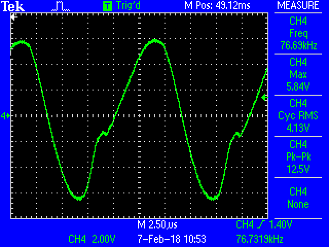
Photo 1. Waveform Across Primary, with Active Arc
Photo 3 shows the waveform across a single turn of wire wound on flyback's core (with active discharge).
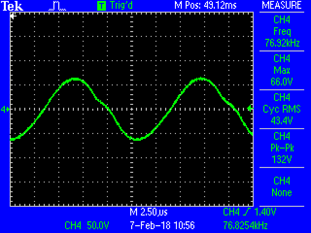
Photo 3. Waveform for a Single Turn Secondary
Photo 4 shows the waveform across a single turn of wire wound on flyback's core, with no arc discharge.
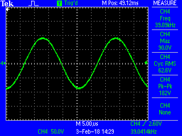
Photo 4. Waveform for a Single Turn Secondary, No Arc Discharge
Page 18
The biggest problem with the basic ZVS driver is that it can "lock up" if the supply voltage is not applied fast enough to kick it into operation. Several videos show this lock up and the high supply currents that result. The way to check for lockup is to monitor the primary for oscillation or to observe the power supply for large currents at startup. Another way to monitor this is to install an LED indicator from each FET drain to ground. IF both LEDs are lit, then the unit is operating properly. If only one LED is lit, the circuit has locked up.
Another way to monitor lockup is to wire an LED and series limiting resistor from each FET drain to ground. If both LEDs light, the ciruit is operating normally;if only one LED lights, the circuit has locked up.
The recommended cure for lockup is to apply the driver voltage quickly, perhaps using a relay. It is common to see the power supply built with a microwave oven transformer that has had its secondary rewound for low voltage and high current. In this "brute force" case is is also common to see the power applied to the driver through a startup relay.
Schematic 3 shows a circuit that is said to prevent lockup and also corrects some other problems with the basic ZVS circuit.
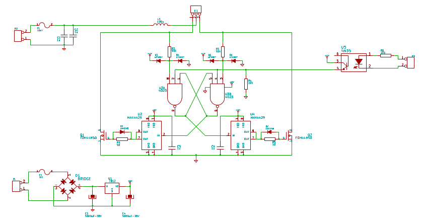
Schematic 3. Improved ZVS Driver
The circuit in Schematic3 was downloaded from the medafire site.
The primary feature of the improved circuit is the use of a set-reset flip-flop to drive the FETs. Thus, each FET is assured of being driven by a phase that is opposite of the the other FET.
The improved circuit also drives the gates with a FET driver, ensuring that the gate charge is driven with a low-impedance source.
The RS flip flop gates are also driven from the two phases with voltage-protected inputs (i.e., using protection diodes and 10K resistors on the gate inputs).
Page 19
Another input of each gate is driven with an opto-isolator to allow the circuit to be turned on and off conveniently.
I have not run across a board that implements the improved circuit. Also, I have not tried this circuit or found any videos showing it in operation.
Page 20
Photo 2 shows the heat sink assembly for the two FETs. The heat sink is held tightly to the backs of the two FETs with some nylon hardware. The FETs are isolated from the heat sink with heat-conductive pads. Thermal transfer is enhanced with heat sink compound on the backs of the FETs and on the surface of the heat sink. A small 12 VDC fan is mounted directly to the heat sink to provide forced air flow.
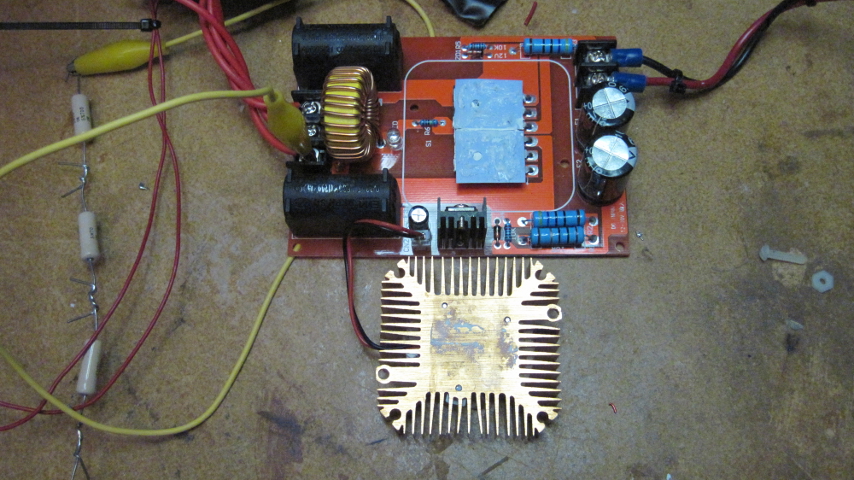
Photo 1. Heatsink Mounting
In doing further browsing for flyback drivers, I found that it is possible to drive a flyback with an electronic ballast for a fluorescent lamp. Ludic Science provides a good example of how to do this: Electronic Ballast Flyback Driver.
Ludic Science also describes how to connect two flyback coils in series: Cascading Two Flyback Transformers
.On eBay, it is now possible to purchase a ZVS driver and a flyback transformer for around $20. I recommend purchasing one of these completed, working units. Even if you are designing your own custom circuit, it is worth observing the layout of a typical ZVS circuit. Here is a typical ZVS & Flyback Driver on Ebay.
Page 21
revised photos, scaled to 640x480, add page numbers, exported photos as 600x480 jpg |
||
major cleanup of schematics, photos and text |
||
updated text according to further measurements and tests on a commercial ZVS flyback module.. |
||
minor editing, removed bogus test link for mp4 video recording. |
||
added electronic ballast addendum |
||
corrected choke current requirements, misc. editing |
||
first edit |
||
initial production release |
||
rough formatting, schematics |
||
Initial version |
Copyright © 2016, Bob Nash.