
The following describes the design, construction and operation of two boards designed to directly interface to the FE-5680A rubidium reference sources.
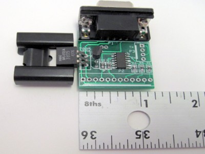
The first of these two boards, called the FE Board (FEBO), plugs into the DB-9 connector on the FE-5680A and provides a power connection, regulated power to the FE-5960A, access to the RS-232 pins and logic buffering of the FE output. An output is also available for an LED "lock" indicator. The basic FEBO board is shown on the left above.
The second of the two boards has the same interface as the basic FEBO module and also has a Phase Locked Loop (PLL) chip to provide an output that is a multiple of the 10 MHz rubidium reference signal. This board, called the FEBO-PLL, is shown on the right above.
For off-line reference, you can download a PDF version of this manual.
Page ii
(BLANK)
Page 1
Page 2
(BLANK)
Page 3
The following describes the design, construction and operation of two modules designed to directly interface to the FE-5680A rubidium reference sources.
One of these modules, called the FE Board (FEBO), plugs into the DB-9 connector on the FE-5680A and provides a power connection, regulated power to the FE-5960A, access to the RS-232 pins and logic buffering of the FE output. An output is also available for an LED "lock" indicator. The basic FEBO module is shown in Photo 1, below.
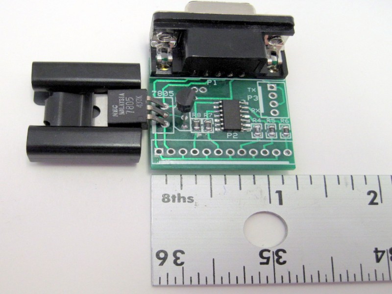
Photo 1 -- Basic FEBO Board
Page 4
The second of the two boards for the FE-5680 has the same interface as the basic FEBO module and also has a Phase Locked Loop (PLL) chip to provide an output that is a multiple of the 10 MHz rubidium reference signal. This module, called the FEBO-PLL, is shown in Photo 2, below.
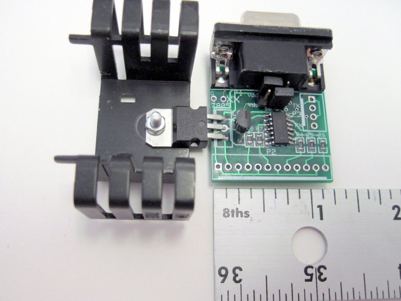
Photo 2 -- FEBO Board with PLL
Page 5
Photo 3 shows the FEBO-PLL module plugged into the back of a FE-5680A.
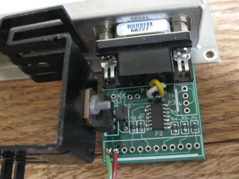
Photo 3 -- FEBO-PLL Plugged into a FE-5680A
Page 6
Photo 4 shows a FEBO being tested while plugged into a FE-5680A.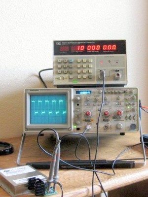
Photo 4 -- FEBO Under Test
Schematic 1 shows the circuitry for both the FEBO and FEBO-PLL boards: the circuitry in the "PLL Option" inset is on the FEBO-PLL module but missing from the basic FEBO module.
We recommend that you download Schematic 1 (a zip file) to have a high-resolution schematic for easy reference in the following discussions.
Page 7
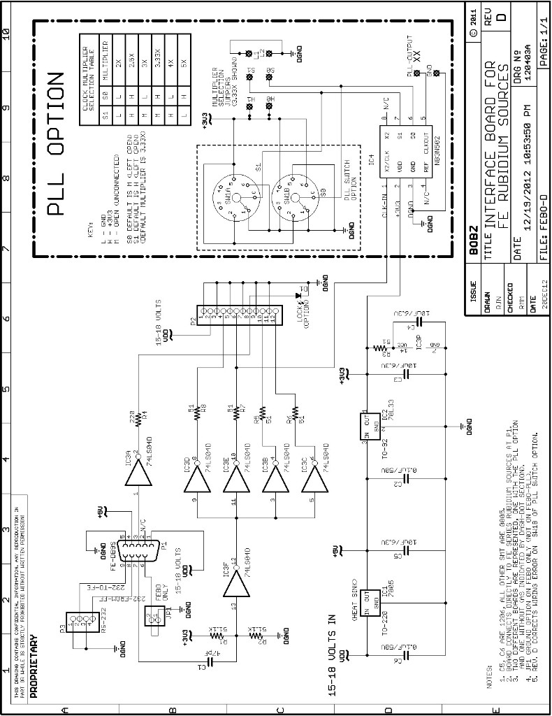
Schematic 1 -- FEBO Interface Board for FE-5960A Rubidium Reference Oscillator
Page 8
For the following, refer to schematic, which shows the components, circuitry and pinouts for the FEBO and FEBO-PLL modules. The Frequency Electronics, Inc. site provides more information on the FE-5680A rubidium reference oscillator.
The Parts List provides additional information about the components used to assemble the board.
The FEBO modules measure approximately 1 1/4 by 1 1/4 inches (32 by 32 mm).
As shown in the schematic, signal connections are available at three points along the board edges. The power input and buffered outputs are available at P2, a 1X12 tenth-inch spaced connector footprint. The RS-232 connections are available at P3, a 1x4 connector footprint with one-tenth inch pad spacing.
For the FE-PLL board, the PLL output is available at two tenth-inch spaced pads labeled "XX" near the 7805 regulator.
Connections to the FE-5680A are made with a DB-9F connector mounted along one edge of the board. Note that the 7805 regulator does require a heat sink -- it is located near a board edge to allow the regulator body and its heat sink to protrude over the side of the board.
The FEBO outputs are available at the board edge connectors and pads, as given above.
The 74HC04 buffer pins are capable of driving 10 LSTTL loads, typically 5 mA. The maximum source and sink current when driving other loads should be limited to no more than 20 mA. Also see the Power section for other limitations.
Page 9
The board was designed to provide a convenient interface to the FE-5680A rubidium frequency reference, including output signal buffering, power I/O and access to the RS-232 pins. For the FEBO-PLL, the board provides a frequency-multiplied output tied to the 10 MHz output.
As shown in the schematic, the design is straightforward with FE-5680A signal I/O connected at the DB-9F connector, P1. Voltage input to the FE-5680A is provided from the power connection at pins 1 and 2 of the 12-pin connector, P2. The RS-232 interface pins are brought out to a separate 4-pin connector footprint.
The lock indicator from the FE-5680A is buffered and connected to pin 8 of the 12-pin edge connector footprint. A current limiting resistor, R4, is wired in series with the output to eliminate the need for an external LED limiting.
The reference output from the FE-5680A is fed through a coupling and bias network to gate IC3F which converts the output to a square wave at logic levels. The output of the squarer gate drives the inputs to four other gates that provides separate buffered outputs to drive external instruments. These buffered outputs are available at P2 pin connections 4, 6, 10 and 12. The power to the 74HC04 is isolated from board transients by a decoupling network consisting of a 51 Ohm resistor and a 10 microfarad capacitor.
For the FEBO-PLL board, one of the buffer outputs also drives the NB3N502 PLL chip that provides a multiplied output (at terminals marked "XX"). The PLL multiplier can be selected by jumpers, as shown in the table within the "PLL OPTION" inset on the schematic. With no jumpers installed, the multiplier rate is 3.33.. . This multiplier value has been tested with a precision 3 MHz oscillator as an input and the resulting PLL output is very close to 10 MHz.
The "PLL OPTION" inset also shows how to use a two-wafer, 6-position rotary switch to select any one of the PLL multipliers.
Note that the FE-5680A datasheet shows pin 6 of the DB9 connector as an optional ground. This pin is grounded on the FEBO-PLL board and is wired to a jumper option (JP1) on the FEBO.
To set up the completed module for operation, plug the board into the FE-5680A and furnish 15-18 Volt power to board at P2, pins 1 and 2 (2 is positive, 1 is the return -- pins 3,5,7,9 and 11 can also be used for the return connection). Once supplied with power, 10 MHz outputs should be available at pins 4, 6, 10 and 12.
Outputs may not be stable until after the unit is locked, as indicated by pin 8 going high. The datasheet says the unit should lock in less than 5 minutes. To connect an LED as a lock indicator, wire the LED anode to the pin 8 connection pad and the cathode to one or more of the odd-numbered pin connections. The on-board current limiter is designed for a red LED. This resistor, R4, may have to be changed for different LEDs and light outputs. The lock indicator wiring is shown on the schematic but the module is not presently shipped with an LED.
Page 10
All boards are tested with the board plugged into a FE-5680A with a power input of approximately 16 Volts DC. The lock and buffer outputs are checked with a scope to verify the lock and buffered 10 MHz outputs. The PLL is also checked for a multiplier of 3.33 (all jumpers removed).
Photo 4 shows a FEBO module under test while plugged into a FE-5680A.
Page 11
![]()
Power to the module is applied between pins 1 and 2 of P2, as shown in the schematic. An on-board 5 Volt regulator feeds 5 Volts to the FE-5680A on pin 4 of the DB-9F connector. The 7805 also acts as a pre-regulator for the 3.3 Volt regulator that powers the 74HC04 buffers and LED driver.
The module operates with an input voltage from 15 to 18 Volts at approximately 700 milliamperes. According to the specifications, power may peak as high as 32 Watts (about 2 Amperes at 16 Volts).
For the FEBO-PLL, the 3.3 Volt output also provides the regulated power it needs.
The 3.3 Volt regulator operates with a nominal input voltage of 5 Volts from the 7805 regulator. But, the worst-case dropout specification for the regulator can be as high as 5.5 Volts. Because assembled modules are functionally tested at 5 Volts before shipment, this worst-case limit shouldn't concern the user. However, this information is provided in the event that a user replaces the 7805 regulator with an external 5 Volt source.
Although the maximum output current for each of the 74HC04 outputs is 20 milliamperes, loading all outputs at this level will exceed the maximum output of the regulator (100 mA). The intent of FEBO is to provide buffered outputs to drive multiple test instruments. If your application requires currents higher than the 100 mA maximum supplied by the 78L33 regulator, use an external 3.3 Volt regulator with a higher output current rating. Connection of an external regulator is beyond the scope of this document.
The 5 Volt regulator is furnished with a heat sink. Do not remove the heat sink unless your installation provides some other method of heat dissipation such as mounting to a chassis with an insulator and heat sink compound.
Page 12
(BLANK)
Page 13
| Part | |||||
| R1,2 | RES 51.1K, 1/8W, 1%, 0805 | Digikey | 541-51.1KCCT-ND |
||
| R3,4,5,6,7,8 | RES, 51R, 1/8W, 1%, 0805 | Digikey | 541-51.0CCT-ND |
||
| R4 | RES, 220R, 1/8W, 1%, 0805 | Digikey | 541-220CCT-ND |
||
| C1 | CAP, 47 pF, 50 Volts, 5%, COG/NPO, 0805 | Mouser | 140-CC501N470J-RC |
||
| C2,6 | CAP, 0.1 uF, 25 Volts, 10%, 0805 | Stock | N/A |
||
| C3,4,5 | CAP, 10 uF, 10 Volts, X5R, 0805 | Digikey | 490-1709-1-ND |
||
| IC2 | REG, 3.3 Volt, TO-92, 100 mA, 250 mW | Digikey | 497-7288-ND |
||
| IC1 | REG, 5 Volt, TO-220, 1 Amp, 10 Watt | Digikey | NCP7805TGOS-ND |
||
| IC3 | logic gate, 74HC04DR2G | Digikey | 74HC04DR2GOSDKR-ND |
||
| IC4 | PLL, NB3N502DG | Digikey | NB3N502DGOS-ND |
||
| PCB | PCB, FEBO, FEBO-PLL | ||||
| P1 | CONNECTOR, DB-9F, board mount | Stock | N/A |
Page 14
major documentation revision, second board run (revised jumper layout). |
||
original documentation, first-run board. |
||
revised per "standard" format with embedded photos, etc. |