
Page 2
The NOIZ module has been superseded by the AGEN module. The documentation in this section is primarily intended for customers who have previously purchased NOIZ modules. The AGEN module produces both white and pink noise using the same algorithm as the NOIZ module. The AGEN module also generates other audio tones and test sounds. The photos in this section showing the white and pink noise outputs and spectrum are identical to those produced by AGEN. Refer to the AGEN documentation for AGEN specifications and a summary of the differences between NOIZ and AGEN.
The following describes the design, construction, operation and use of the NOIZ White and Pink Noise Generator module. The primary use of the module is to generate simultaneous white and pink noise signals for audio testing.
As shown in Photo 1, the white noise signal is at logic levels. Photo 2 shows a narrow spectrum (25 kHz per horizontal division) view of the white noise output. The wide spectrum (250 kHz per horizontal division) output of the white noise is shown in Photo 3.
As shown in Photo 4, the pink noise is at a level of a few tens of millivolts for input to an audio system. Photo 5 shows a wide spectrum (250 kHz per horizontal division) view of the pink noise output.
Page 3
For the following, refer to Schematic 1 titled "NOIZ WHITE AND PINK NOISE GENERATOR." The schematic shows the components, circuitry and pinouts for the module. User's with older NOIZ modules with only 6 I/O pins please refer to the Schematic 2. You can download both NOIZ schematics as a zip file.
The Parts List provides additional information about the components used to assemble the module.
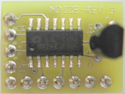
The module measures approximately 9/16" by 13/16" (15 mm by 20 mm). As shown in the schematic, signal connections are available at a single row pin header, J3. Power connections are brought out to a two-pin header, J1. An third 6-pin header, J2, provides connections to the noise module's microprocessor pins and is currently not used except for testing. The microprocessor's system clock, at a frequency of approximately 24.5 Megahertz, is available at pin 3 of this connector.
![]()
The module provides two simultaneous outputs, one for pink noise and one for white noise. Other outputs are wired to module pins but are reserved for factory testing and future features.
The white noise output, available on J3/4, is directly connected to one of the microprocessor's port pins and is capable of sourcing or sinking up to 100 milliamperes (also reference the Power section). The pink noize output is at a level of a few tens of millivolts and is at a relatively high impedance level (it is driven through a 6.8K resistor from a microprocessor output).
Page 4
The white noise output is derived from a 31-bit pseudo-random noise generator implemented in software.
The pink noise output is also derived from the same software generator as the white noise signal but the white noise is first filtered by a "pinking" network before it is routed to the module's pink noise output (see the section labeled PINKING NETWORK on the schematic.)
To set up the module for operation, it is necessary only to supply it with power. Once supplied with power in the range of 5.2 to 16 Volts, white and pink outputs are continuously available (also see the PIN/PORT MAPPING table on the schematic).
The following sections describe power connection and verification procedures.
All module outputs are verified on a test fixture before shipment. Outputs are checked for waveform integrity and level with a Tektronix TDS 2014 oscilloscope. The pink noise output is also visually checked by observing correct frequency rolloff with the oscilloscope's FFT display.
Page 5
![]()
An on-board 3.3 Volt regulator provides stable regulated power to the module. As shipped, the module operates with power inputs from 5 to 16 Volts. To configure the module for operation, connect the negative input of the power supply (i.e., ground reference) to J1/1 and connect the positive supply voltage to J1/2 (also see the polarity caution below).
Once the proper input voltage is applied to pins J1, the operation of the regulator can be verified by measuring the voltage between ground and the output pad for the regulator. This pad is labeled "out" on the module. The power can also be verified by carefully probing the voltage on pin 3 of the microprocessor. The measured regulator output voltage should be close to 3.3 Volts.
Note that the module may operate with an input voltage as low as 5 Volts, but the worst-case dropout specification for the regulator is 5.5 Volts. because modules are tested with a supply that measures just below 5.2 Volts, the module will operate at this lower voltage but operation at voltages lower than this test voltage is not guaranteed.
Module quiescent current draw is approximately 12 milliamperes. Total regulator dissipation is 250 milliwatts and the maximum regulator output is 100 milliamperes. The regulator is both current and temperature limited in the event of output overload (e.g., too heavy a load on the white noise output or inadvertent shorting of the unused port pins on J2 and J3).
Be aware that the total regulator dissipation is 250 milliwatts and the maximum regulator output is 100 milliamperes. We recommend that the dissipation be kept below half the dissipation limit and below the maximum current limit. The regulator is both current and temperature limited in the event of output overload.
Page 6
| Part | |||||
| R1 | RES, 6.8K, 1/8W, 1%, 0805 | Digikey | 541-6.8KCCT-ND |
||
| R2 | RES, 3K, 1/8W, 1%, 0805 | Digikey | 541-3.00KCCT-ND |
||
| R3 | RES, 1K, 1/8W, 1%, 0805 | Digikey | 541-1.00KCCT-ND |
||
| R4 | RES, 300R, 1/8W, 1%, 0805 | Digikey | 541-300CCT-ND |
||
| C1,6 | CAP, ceramic, 1 uF, 25 Volts, Y5V, 0805 | Digikey | C2012Y5V1E105Z/0.85 |
||
| C7 | CAP, 10 uF, 10 Volts, X5R, 0805 | Digikey | 490-1709-1-ND |
||
| C2 | CAP, 0.27 uF, 16 Volts, 10%, 0805 | Mouser | 77-VJ0805Y274KXJRBC |
||
| C3,4 | CAP, 0.047 uF, 25 Volts, 10%, 0805 | Mouser | 81-GRM40X473K25D |
||
| C5 | CAP, 0.033 uF, 50 Volts, 10%, 0805 | Digikey | 490-1660-1-ND |
||
| U1 | voltage regulator, 3.3 Volt, TO-92, 100 mA, 250 mW | L78L33 |
|||
| U2 | microprocessor, C8051T602-GS OTP, pre-programmed | Digikey | 336-1655-5-ND |
||
| PCB1 | PCB, NOIZ, revision 3 | ||||
| PHD1,2 | 12-pin header, SIL, breakaway (13 pins used) | FRYS | PLS-40S-P5 |
original circuit, revision B of the schematic |
||
brought out unused processor pins, revision 3 of board, revision C of the schematic |