The PRUBY module that provides a PLL interface for rubidium frequency references such as the LPRO-101 and FRS-C products manufactured by EFRATOM Ball, Inc.. The module conditions the ten megahertz (MHz) signal from the reference and provides both a square wave reference output and a frequency-multiplied output. The multiplied output is phase-locked to the reference input and can be set with on-board jumpers to 2, 2.5, 3, 3.33, and 4 times the reference input signal (e.g., 10 MHz).
The module can be used to condition, lock and multiply other input frequencies, provided that the module limits are met. Input voltages are typically 1 Volt Pk-Pk.
Other module features include an on-board 3.3 Volt regulator for the PLL chip, a 3.3 Volt output and a FET driver for an LED (e.g., for a lock indicator). An on-board zener diode can be enabled to support higher power supply voltages such as those typically available from rubidium references.
Page ii
(BLANK)
Page 1
Page 2
The following describes the design, construction, operation and use of a module that provides a PLL interface for a rubidium frequency reference (PRUBY). The primary use of PRUBY is to condition the ten megahertz (MHz) signal from a rubidium reference oscillator and provide a frequency-multiplied output that is locked to the reference. The PRUBY module was designed for use with with the LPRO-101 and FRS-C rubidium frequency reference modules manufactured by EFRATOM Ball, Inc.
The PRUBY module consists of a PLL chip and a voltage regulator that converts the input reference signal to a logic level and multiplies it according to on-board jumper settings. The PLL multiplied output, typically 25 MHz, can be used as a stable phase-locked output that is referenced to the input source.
The module's PLL can be used for other applications requiring signal conditioning and frequency multiplication but this usage is outside the scope of this document.
For the following, refer to the schematic of the module, Figure 1, titled "PLL MULTIPLIER FOR RUBIDIUM REFERENCE."
The schematic shows the components, circuitry and some operational information for the module. For example, the schematic includes a table for PLL jumper options and bottom-side component placement for the PCB. The Parts List provides additional information about the components used to assemble the module.
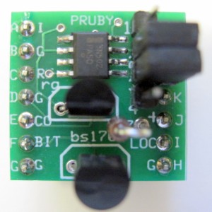
As shown in the photo of the module, it is relatively small, measuring approximately 3/4 by 3/8 inches (19 X 19 mm).
Signal connections are provided on two single row pin headers in a DIP format. A 7-pin header is located on one board edge and a 6-pin header on the other edge. The header I/O connections are labeled "A" to "K" for easy reference. Header pins are spaced one tenth of an inch apart and the header rows are spaced 0.6 inch apart. This allows the module to be used with in-line sockets or wired on a protoboard.
Some of the header pins are used to select clock multiplier options. These jumper connections are labeled "5" and "6" to correspond with jumper pin pads placed on the board interior. The interior jumbpers are labeled "1", "2", "3" and "4" to distinguish them from I/O connections and correlate them to the connections labeled "5" and "6."
The module includes a P-channel MOSFET that can be wired to drive an LED to indicate that the rubidium reference is locked. As shown in the schematic, the lock output from the rubidium reference connects to the MOSFET gate at module pin "F", which is also functionally labeled "BIT." The LED current limiting resistor, R4, is located on-board, as indicated on the schematic in the "BOTTOM PARTS PLACEMENT" inset. The limiting resistor was selected for a current of approximately 5 milliamperes. For different currents or output devices, R4 can be replaced using the parts placement diagram as a guide.
The output of the PLL can drive up to 25 milliamperes, subject to the limitations of the voltage regulator, as discussed in the Power section.
Page 3
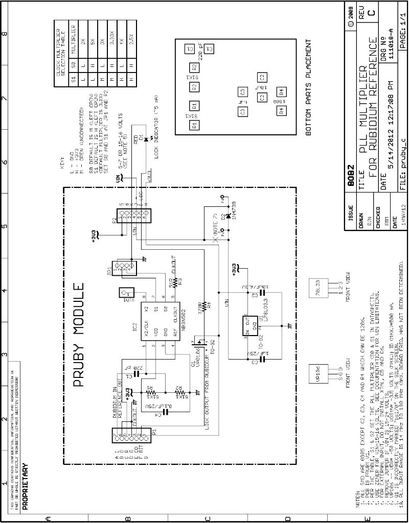
Figure 1 -- Schematic of PRUBY PLL Multiplier
Page 4
The input conditioning circuit was developed by experimenting with the input conditioning used for DECUS. The clock input to the PLL was biased to 50% of the supply voltage and capacitively coupled to the input signal from the rubidium oscillator. This approach works reliably but requires a somewhat larger coupling capacitor than used for DECUS.
The input circuit works with the typical input from an LPRO rubidium reference, which is approximately 0.55 Volts RMS. The circuit also works reliably with inputs ranging from approximately one Volt peak-to-peak (Pk-Pk) to several Volts Pk-Pk. The input was not rigorously characterized versus frequency, but appears to operate reliably in the range of 5 to 20 MHz.
The module is designed so that all pins are on 0.1 inch centers to facilitate protoboard wiring or plugging into a breadboard socket. If used with a breadboard socket, note that higher frequency signals may be degraded by capacitance between breadboard socket rows. This is especially true for higher frequency PLL outputs.
To set up the module for operation, it is necessary only to supply it with power and an input signal. Once set up for operation, outputs are continuously available at the lettered output pins, as shown in Figure 1. The power and I/O connections are described below.
The following sections describe power and signal requirements, other module connections and test procedures.
Module outputs are tested before shipment with an LPRO-101 or FRS input source. Outputs are checked for waveform integrity, level and frequency with a Tektronix TDS 2014 oscilloscope.
Page 5
Apply the input signal between pin "A" (RUBIDIUM IN) and pin "B" (ground), as shown in Figure 1.
The input conditioning circuit is designed to be compatible with the LPRO-101 specifications with a typical input signal of 0.55 Volts rms (approximately 1.5 Volts p-p). Figure 2 shows a typical LPRO input (blue trace on the bottom -- top trace is the DECUS conditioned output). Note: The input may not operate reliably for signal inputs under one Volt Pk-Pk. Inputs as high as 6 Volts peak to peak have been used but are not recommended for routine operation.
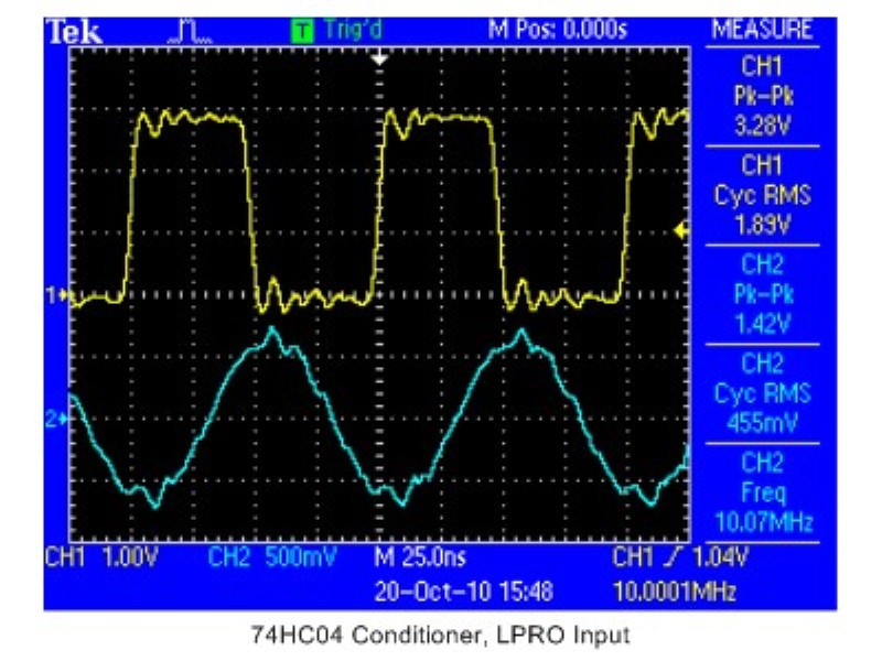
Figure 2 - Scope Photo of Typical LPRO Input (bottom trace)
Page 6
The module provides a reference output on pin "C", which is also functionally designated "R" for "Reference." This is a 10 MHz conditioned output.
The PLL output appears on pin "E", which is also functionally labeled "CO" for "Clock Output." This is the multiplied output, as selected by the jumpers 1-6. With no jumpers installed, the PLL output at "E" is 33.33.. MHz. Other multipliers can be selected by leaving jumpers unconnected or wiring them low or high, per the table in Figure 1.
For example, to set a multipier of 5, wire pad "2" to pad "1" (X1=L) and wire pad "3" to pad "6" (X0=H). The jumpers are set up so that all "H" and "L" options can be set by wiring pads "2" and "3" to adjacent pins (i.e., a horizontal jumper for "H" and a vertical jumper for "L").
You can connect a red LED (not furnished) between pin "I" (LOC) and ground (e.g., pin "K") to act as an activity indicator or, more commonly, as a "lock" indicator for a rubidium reference oscillator. The indicator LED is driven from a P-channel MOSFET (FET) so that an "active low" logic input at pin "F" (BIT) will turn the LED on.
With the 370 Ohm resistor shown, the LED should draw approximately 5 milliamperes. This relatively low current is set because to avoid additional regulator dissipation. A future board revision may drive the LOC output from VIN and provide a through-hole resistor to provide more drive flexibility. For now, the current limiting resistor, R4, must be replaced with an 0805 SMT part to adjust the LED current. Also see the Power section below for dissipation limitations.
Page 7
![]()
An on-board 3.3 Volt regulator provides stable regulated power to the module. As noted below, this limits the input voltage ranges.
The units are shipped with a shorting jumper across D2, the zener diode used for higher voltage operation. For 5 to 7 Volt operation, apply power between pin "J" (VIN) and pin "K" (ground).
To operate from 15 or 16 Volts you can use the on-board 9.1 Volt, 1 Watt, zener diode (D2) to drop the input voltage to the regulator. To use this zener, remove the shorting jumper across the diode by cutting the looped and soldered leads on the bottom of the board. The module can be operated at 24 Volts by adding another 9.1 Volt, 1 Watt zener in series with the power input (pin "J").
Once the proper input voltage has been selected and configured, the operation of the regulator can be verified by measuring the voltage betweeen ground (pin "K") and the the regulator output (pin "H"). The measured voltage should be within a tenth of a Volt of 3.3 Volts. If the regulator is hot or if the output voltage is not within specification, it is likely that the input voltage is too high or too low or the current through the regulator is too high.
As shipped, the module operates down to 5 Volts. But, note that the datasheet gives a typical (not maximum) dropout voltage of 1.7 volts. Thus, the input voltage should typically be 1.7 Volts (or more) above the output voltage. The nominal output voltage of the regulator is 3.3 Volts but we have seen outputs as low as 3.2 and as high as 3.4 Volts.
The datasheet specifies a worst-case minimum input voltage of 5.5 Volts. This information may be useful if you have to replace the on-board regulator or need to remove it and use an off-board regulator.
Because the modules are tested with a 5 Volt supply, operation at this voltage is assured. But, operation at lower voltages is not guaranteed.For operation slightly below 5 Volts, the user should verify the operation of the module before assuming that it will operate correctly. Also, the module should be re-tested if the on-board regulator is replaced or if the on-board regulator is replaced with an external regulator.
Page 8
When operating at 3.3 Volts, the module's quiescent current draw is approximately 30 milliamperes. Although the on-board 3.3 Volt regulator can handle up to 100 milliamperes, its dissipation is limited to 250 milliwatts.
Any drive current supplied by the outputs adds to the regulator current and thus increases total dissipation. This is not normally a problem, but the information in this section can be used to calculate the impact of higher output loading.
For either high or low input voltages, be aware of regulator dissipation limit of 250 milliwatts.
For example, using the zener and the maximum input voltage of 16 Volts, the regulator dissipates approximately [(16-9.1-3.3) Volts]*[30 milliamperes] = 110 milliwatts. Operating at 7 Volts, the regulator dissipates [(7-3.3 Volts)]*[30 milliamperes] = 111 milliwatts. Current for the indicator can add to this dissipation.
Although the dissipation can probably be pushed up a bit if there is adequate cooling, operation at higher voltages should be avoided. We have used units with input voltages of 9 Volts, but the regulator dissipation in this case is high (i.e., about 170 milliwatts). Ideally, the regulator should not dissipate more than approximately half of its rated power of 250 milliwatts.
The regulator is both current and temperature limited in the event of output overload (e.g., due to high input voltages or additional output loading). Operating at input voltages near the maximum current or dissipation limits may cause the regulator to partially or intermittently shut down, thus affecting the operation of the PLL chip.
Page 9
| Part | |||||
| R1,2 | RES 51.1K, 1/10W, 1%, 0805 | Mouser | 667-ERJ-6GEYJ510V |
||
| R3 | RES, 51R, 1/10W, 1%, 0805 | Digikey | 541-51.0CCT-ND |
||
| R4 | RES, 370R, 1/10W, 1%, 0805 | Mouser | 667-ERJ-6ENF3700V |
||
| C1 | CAP, 220 pF, 200 Volt, NPO, 0805 | N/A | stock |
||
| C2 | CAP, 10 uF, 6.3 Volt, X5R, 0805 | Digikey | PCC2225CT-ND |
||
| C3 | CAP, 1 uF, 25 Volt, X5R, 0805 | Digikey | PCC2319CT-ND |
||
| C4 | CAP, 0.1 uF, 50 Volt, 5%, X7R, 0805 | Digikey | 478-3352-1-ND |
||
| D2 | zener diode, 1N4739, 9.1 Volt, 1 Watt, DO41 | Digikey | 1N4739ADICT-ND |
||
| U1 | voltage regulator, 3.3 Volt, TO-92, 100 mA, 250 mW | L78L33 |
|||
| IC2 | PLL, NB3N502 | Mouser | 863-NB3N502DG |
||
| PCB1 | PCB, PRUBY | ||||
| P1,2 and JP1 | 12-pin header, SIL, breakaway | FRY'S | PLS-40S-P5 |
Page 10
Original circuit, board revision set at "V2" |
||
schematic revision C, corrected wiring error at I and H. |
||
Reformatted to be consistent with DCON format. Misc. editing, in-text photos, etc. |