Page 2
Page 3
The following describes the design, construction and operation of the Radio Frequency Amplifier (RF-Amp) board, a single-transistor Class-A radio frequency amplifier.
The amplifier can be used in a number of projects to buffer and amplify outputs from devices such as Direct Digital Synthesizer (DDS) chips. The board was initially produced to amplify the output of the 9833 DDS chip. The board was also intended for Amateur Radio applications (e.g., a buffer amplifier for a VFO).
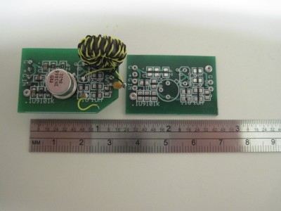
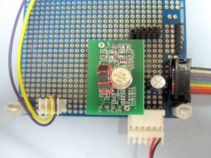
Photo 1 shows the bare board and a board populated with all components except the optional output filter network. The board shown uses a bifilar wound 4:1 output transformer (as shown on the schematic and mentioned below).
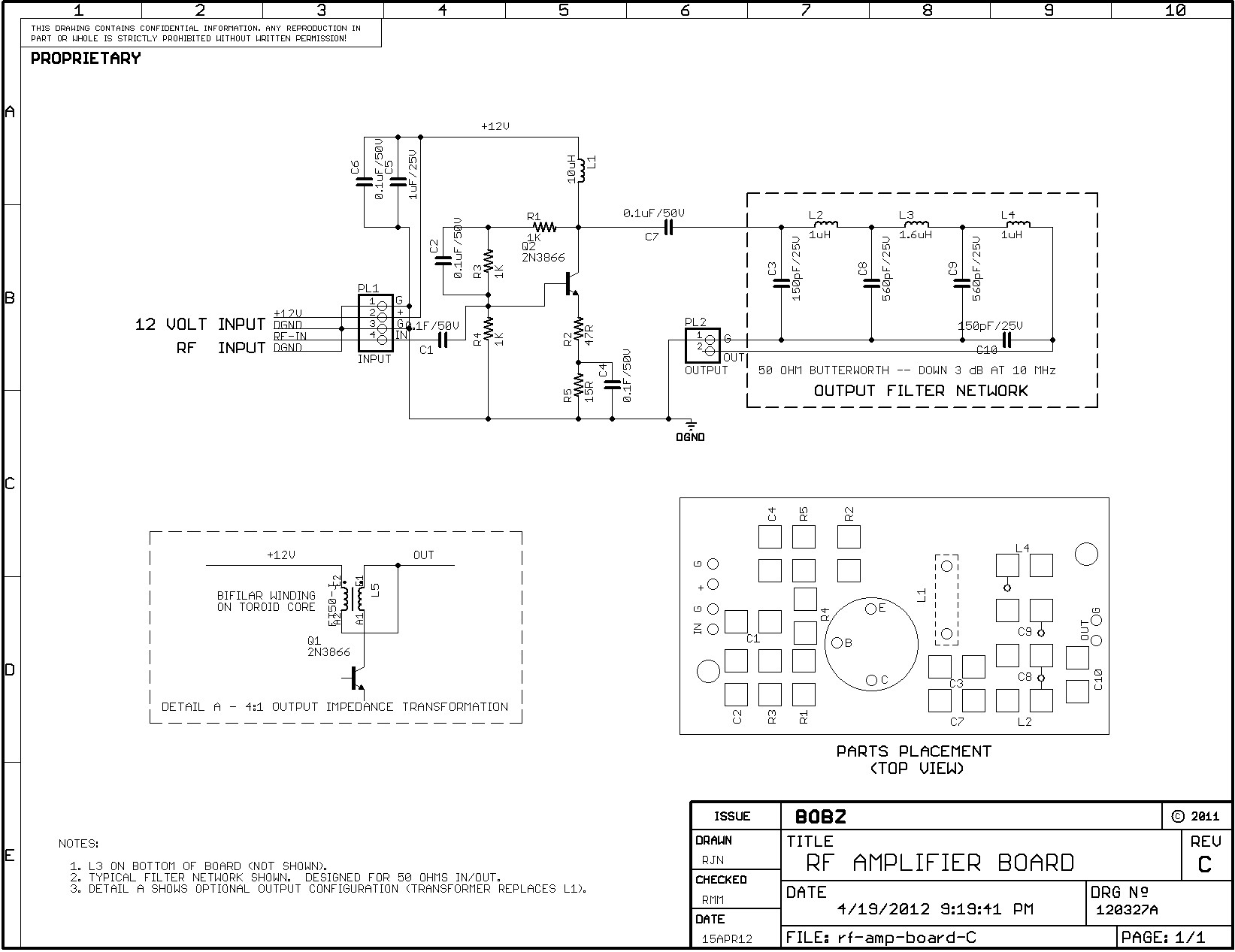
Schematic 1 shows the RF-Amp circuitry and a typical configuration of the optional output network. Note: with the given filter network, frequencies above 10 MHz are greatly attenuated.
Page 4
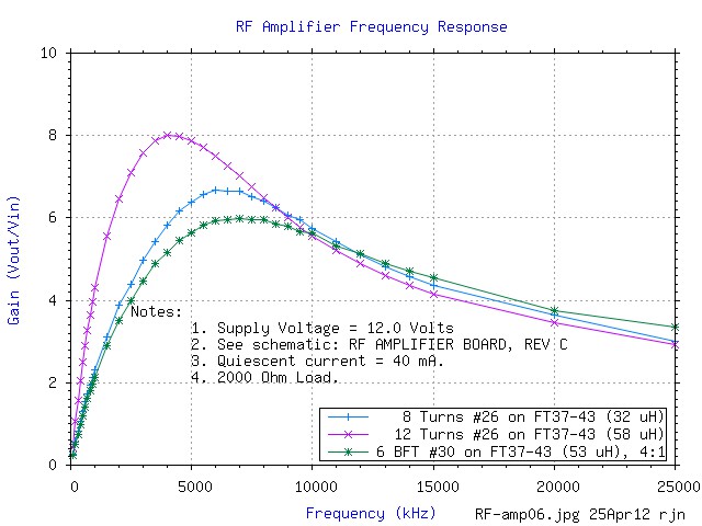
The schematic shows the board's component layout, circuitry and connection points. The amplifier provides a voltage gain of approximately 16 to 18 dB. Photo 2 shows a gain vs. frequency plot of the basic amplifier board with an output optimized for the 3-10 MHz range (2000 Ohm load). Shown on this plot are the results for three different transformer windings, as follows:
You can download Schematic 1 and you can download RF-AMP gain plots.
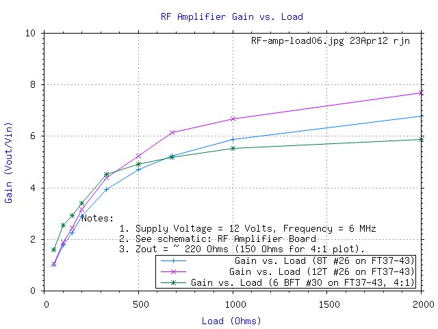
Photo 3 shows a gain vs. load plot of the basic amplifier board for the three windings given above. These plots show that the output impedance of the amplifier is approximately 220 Ohms without the 4:1 winding. With the impedance transformer, the output impedance is reduced to approximately 150 Ohms.
The reduction over the 12 turn transformer is not 4:1 probably because the differences between the collector impedances for the two different transformers; the collector loading for the two transformers is comparable, but not exact.
With the 4:1 transformer, a 2000 Ohm load and a frequency of 6 MHz, the voltage ratio between the collector and secondary of the transformer was (4220 mV rms)/(2210 mV rms)=1.91. This is very close to the expected ratio of 2:1 (impedance transforms as the square of the voltage).
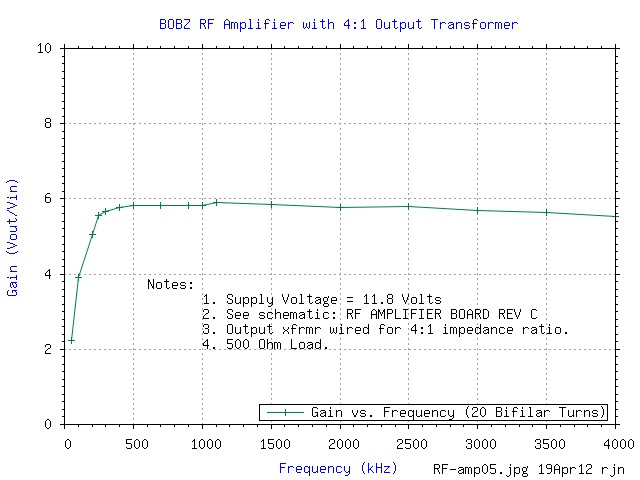
Photo 4 shows a gain vs. frequency plot of an amplifier board optimized for operation at a lower frequency (e.g., 300-400 kHz) connected with the optional 4:1 output transformer shown in the schematic.
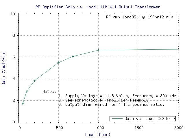
Photo 5 shows a load plot for the same low frequency amplifier. The output impedance, as determined by the point that the load reduces gain by one-half, is approximately 100 Ohms.
The Parts List provides additional information about the board components.
Because the available supply voltage was only 11.8 Volts for the low frequency plots, the gain will be somewhat larger with a full 12 Volt supply. Also note that the amplifiers use a FT50-J core, as noted. This core is good for operation at a few hundred kilohertz to several megahertz. For higher frequency operation, the type 43 core gives better results.
The module measures approximately 1 1/4 by 7/8 inches (32 X 23 mm). As shown in the schematic, signal connections are available at two single row pin headers located on the two short edges of the board. A four-pin connector provides power and input connections to the board and a two pin connector provides the output connections.
As shown on Schematic 1, the input signal is applied on PL1, between pin 4 and pins 1 and 3 (grounds). The nominal input signal level is 500 mV rms.
As shown on the schematic, an optional filter network can be installed between the output of the amplifier (at C7) and the output terminals. If the output filter is not used, a short jumper must be installed from C7 to the output terminal at PL2. This jumper is shown in Photo 6 that shows the amplifier board mounted on a test jig.
Page 5
![]()
Power is applied between pins 2 (+12 Volts) and pins 1 and 3 (grounds). Two on-board filter capacitors provide local power bypassing. For applications with other sensitive circuitry, a separate 12 Volt supply or regulator are recommended.
The module is designed for operation at 12 Volts. It will operate at other voltages. But, operation at other voltages may require checking the output (e.g., for distortion and amplitude) over the frequency range of interest. Operation at other voltages may be improved by scaling the bias network up or down.
Photos of the module show the transistor without any heat-sinking. We recommend putting a heat-sink "hat" or clip for dissipation levels that are near the transistor limits (e.g., 1 Watt or 3 Watts, depeneding on transistor type). In general, any dissipation over 500 milliwatts should have some heat sink attached to the transistor can and some air flow.
Page 6
The amplifier wasn't designed so much as it was adapted from similar circuits appearing in Amateur Radio publications. For example, refer to "Experimental Methods in RF Design", by Hayward, Campbell and Larkin for several similar circuits. A good starting point is Chapter 6, "Transmitters and Receivers", especially the sections on VFO amplifiers.
The design is relatively straightforward with R1, R3 and R4 providing base bias. To help linearity, R2 provide some negative feedback. The quiescent DC operating current is set by R2 and R5. The bias is approximately 40 milliamperes. Output coupling is provided by C7.
Optionally, the output can be filtered by the output filter network. The schematic shows a typical filter that starts rolling off at 10 MHz. The output filter network was designed using the Elsie® filter design software from Tonne Software)
To connect the board for operation, it is necessary only to supply it with power and an input source. Once supplied with 12 Volt power, as described above, the input signal can be applied. An input signal applied to the board without power, does no harm if levels are maintained within a few hundred millivolts.
The input is typically near 0.5 Volt rms and can be applied to the input connector, PL1, as shown in Schematic 1.
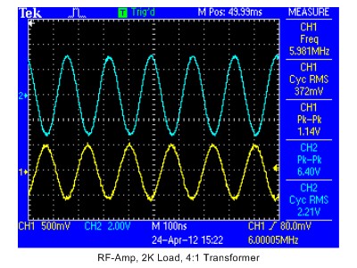
With L1 wound as given in Photo 2 and a signal frequency of approximately 5-7 MHz, the output should be approximately 4 Volts p-p.
Photo 7 shows the input and output signals with a light load and a 4:1 transformer.
The RF-Amp boards are assembled and tested, except for the output filter network. On request, boards can be shipped with the network shown. For those installing their own filter network, refer to the Assembly Guide on the main menu for SMT soldering tips.
Page 7
The following parts list is for the RF-Amp board populated with the filter network shown on the schematic.
| Part | |||||
| R1, R3, R4 | RES, 1K, 1/8W, 1%, 0805 | Digikey | 541-1.00KCCT-ND |
||
| R2 | RES, 47R, 1/8W, 1%, 0805 | Digikey | P47.0CCT-ND |
||
| R5 | RES, 15R, 1/8W, 1%, 0805 | Digikey | P15.0CCT-ND |
||
| C1, C2, C4, C6, C7 | CAP, 0.1 uF, 25 Volt, Y5V, 0805 | Digikey | 490-1726-1-ND |
||
| C5 | CAP, ceramic, 1 uF, 25 Volt, Y5V, 0805 | Digikey | 490-1731-1-ND |
||
| C3, C10 | CAP, 150 pF, 50 Volt, 5%, COG/NPO, 0805 | Digikey | 490-3315-1-ND |
||
| C8, C9 | CAP, 560 pF, 100 Volt, 5%, NPO, 0805 | Digikey | 490-1612-1-ND |
||
| L1 | 58 uH, 12T #26 on Amidon FT37-43 | Amidon | |||
| L2, L4 | 1 uH, 0805 | Digikey | 587-1688-1-ND |
||
| L3 | 1.6 uH, 0805 | Digikey | |||
| Q1 | Transistor, 2N3866 | Mouser | 610-2N3866 |
||
| PCB1 | BOBZ RF-AMP PCB | BOBZ |
original board layout, Rev. C of the schematic |