The DCON (Dds CONtroller) DDS controller is a microprocessor-based module that provides a simple way to control up to two Direct Digital Synthesizer (DDS) modules from a serial data link. The serial data link can consist of a serial terminal, the serial output from a microprocessor (such as a PIC or Arduino) or the serial output of a PC program.
The controller is designed to operate with inexpensive DDS modules using the Analog Devices 9850 or 9851 chips. These are widely available on the internet. The 9850 DDS modules are commonly available for under ten dollars.
The controller responds to commands entered on its serial input. Most commands consist of one or two ASCII characters. Longer sequences allow setting of operational data such as frequency. Error conditions are fed back to the control processor or user with both a hardware output and serial error responses.
To simplify setup and use, operating parameters can be saved to flash memory for startup in a known state. With only a few commands, a module can be set to automatically come up as a fixed-frequency oscillator. An extensive command set provides the flexibility needed for more demanding applications such as setting up two modulules to operate at variable frequencies under control of a microprocessor.
For off-line reference, you can download a PDF version of this manual.
Page ii
(BLANK)
Page 1
Page 2
Page 3
Page 4
(BLANK)
Page 5
The DCON (Dds CONtroller) controller is a microprocessor-based module that provides a simple way to control up to two inexpensive Direct Digital Synthesizer (DDS) modules from a serial data link. The serial data link can consist of a serial terminal, the serial output from a microprocessor such as a PIC or Arduino or the serial output of a PC program.
The DCON module responds to simple ASCII character commands. Most commands consist of one or two ASCII characters. Longer sequences are needed only to specify operational parameters such as frequency. The commands are listed in the Command Summary Table. The following section provides a detailed functional overview of DCON capabilities.
The controller is designed to operate with inexpensive modules based on the Analog Devices 9850 or 9851 DDS chips. The 9850 modules are commonly available on EBay for under ten dollars. The 9851 modules are more expensive and are in the range of twenty dollars. Controller commands are available to switch between 9850 and 9851 modules.
The controller has features that simplify its operation as a peripheral to a microprocessor or a PC. These include both hardware and serial link responses to error conditions. Commands are also provided to reset error conditions and to reboot.
To simplify setup and use with an external system or for custom applications, operating parameters can be saved to flash memory. An extensive command set provides flexibility in setting up one or two modules as Variable Frequency Oscillators (VFOs) or more demanding applications that require frequent adjustment of frequencies.
Documentation is available on a CD (with purchase) or free at the Kibler Electronics site. The documentation at this site describes the operation of the controller in detail and includes documentation for other products that may be used with the DCON module (e.g., interfaces to rubidium reference sources, frequency multipliers, amplifiers).
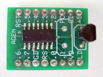
The DCON module is based on the AGEN microprocessor module used for other BOBZ products. For DCON, the AGEN Module is populated only with a microprocessor, a 3.3 Volt regulator and reset circuitry. Firmware for the DCON application is loaded into the chip to provide the DCON functions. But, because the DCON Module can be programmed with the ADEV Development System, users with this programmer can install updates and custom upgrades from downloaded files.Page 6
Controller features include the following:
Page 7
Thus, the DCON Module can be used for projects that require a "ready to use" serial controller for projects using one, two or more DDS modules.
The controller measures approximately 3/4 by 7/8 inches (19 by 23 mm). As shown in the Schematic, signal connections are available on two single-row pin headers located along the board's long edges.
The controller module consists of an ATAR target board (labeled "AGEN") that is populated with a C8051F300 chip without an external crystal. The chip can be reprogrammed using the ADEV Development System, the Silicon Laboratories (SL) Debug Adaptor and Integrated Development Environment (IDE). However, the DCON module is delivered pre-programmed and tested with default values that allow immediate use.
Page 8
Before proceeding, we recommend that you download DCON schematics as a zip file and print them out. The downloadable schematics are high resolution files that, when printed out, are easier to read than the schematics embedded in the body of this manual. Also, because these schematics are cited often, it is more convenient to reference the printed schematics than to frequently page back to them.
Figure 1 is a schematic of the DCON dual DDS interface. It shows how the DCON Module connects to two DDS modules and to typical serial interfaces.
The schematic also shows how to wire a 10-pin connector for use with the Silicon Laboratories (SL) Debug Adapter. This allows the DCON Module to be reprogrammed using the Debug Adapter and the SL Integated Development Environment without having to disconnect it from the two DDS modules.
Figure 2 is a schematic showing a DCON development configuration with two DDS units of different manufacture. One of the boards is connected via a cable external to the DCON motherboard. This schematic shows how the Test/Programming Board connects via an adapter board to a DDS module that has header connections that are not arranged in a DIP configuration.
The Parts List provides additional information about the components used to assemble the board.
Page 9
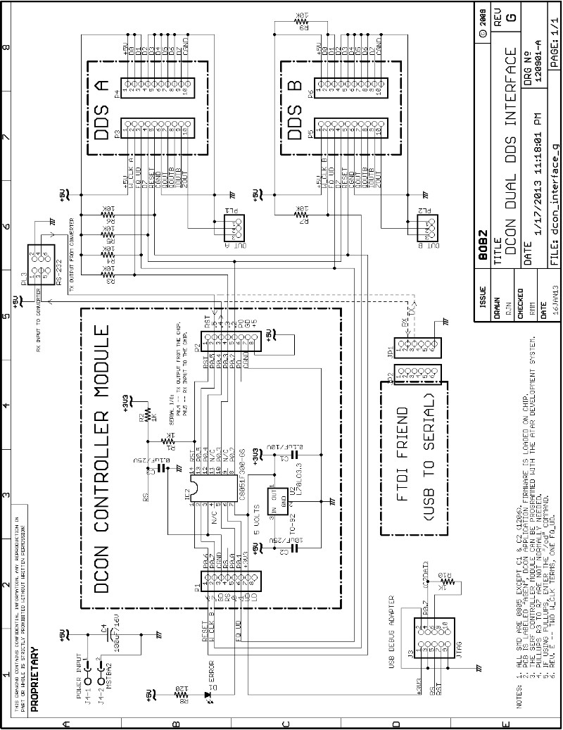
Figure 1 -- Schematic of DCON Dual DDS Interface
Page 10
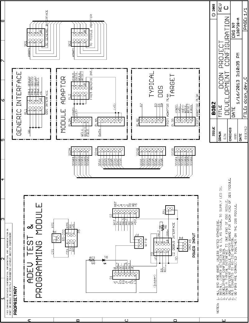
Figure 2 -- Schematic of a DCON Development Configuration
Page 11
All processor port pins are available at the two 8-pin edge connectors, as are power input (e.g., 5 Volts), power output (3.3 Volts) and reset (the pin labeled "RS", P1/4). Note that a pin labeled "RST" is also available but it should not be used to reset the processor: it is used only for chip programming.
Although a description of the capabilities of the SL C8051F300 microprocessor is beyond the scope of this document, one important feature of the chip is that the port pins can sink up to a maximum of 100 milliamperes when configured as push-pull outputs (also see the Power section).
Page 12
The following are the basic design objectives for the DCON controller:
To set up the completed module for operation, it is first necessary to supply it with power by connecting 5 Volts between the "+5" pin and the "GD" (ground) pins.
![]()
In the following, the controller pin numbering follows that shown in Figure 1. Controller connections appear on two stake-pin headers, P1 and P2. Hereafter, pin notation for these connectors is simplified. For example, header P2, pin 7 is denoted "P2/7" and header P1, pin 2 is "P1/2".
Apply +5 Volts to P2/8 and connect ground to P1/3 and P2/7. If you are socketing the module, it is best to check for correct voltages on the socket pins before inserting the module. To simplify this verification, power connections are silk-screened on the top of the module.
The Power section provides more detailed information about module power connections and the limitations on the 3.3 Volt regulated power at P1/7.
Page 13
Next, connect the module to a serial port. A simple way to do this is to use a USB to serial adapter such as that provided by the "FTDI Friend" from AdaFruit Industries. Connections to the "FTDI Friend" are shown in Figure 1.
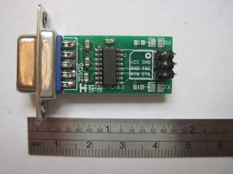
This schematic also shows connections to a RS-232 converter commonly available on the internet. Figure 3 shows one of these converters that was purchased for about three dollars. The connections for this adapter are also shown in Figure 1 (see the top center of schematic).
Page 14
We like the FTDI Friend for the serial connection because it requires only a few simple connections and shows the data directions for the Tx and Rx connections on the board's silkscreen. Another unit that we like is the FT232R Breakout Board from sparkfun Electronics.
Although we use both products, the Breakout Board, because of its added functionality, has a slightly larger footprint and number of pins. Both of the units use the FTDI USB to serial adapters. These work very reliably on both our Windows and Linux machines, reportedly because the drivers are well-designed. Figure 4Shows both the FT232R Breakout and the FTDI Friend boards. The Figure shows both connected to a development board. This is to illustrate the connection points for the adaptors -- connect either one or the other.
Once the controller is wired to power and an RS-232 connection, test it by bringing up a terminal application, such as Hyperterm, Procomm, PuTTY, or Minicom (Linux). Configure the terminal program for 9600 baud with 8 data bits, no parity and one stop bit. Also disable local character echoing. When configured and connected properly, typing a command elicits a response from the processor.
Connect the configured terminal and apply power to the controller. When power is first applied to the controller, it outputs a "!" to signal a reboot. An external controller can monitor for this character to verify system power cycling or a forced reboot (e.g., using the "r" command). To test the controller, enter the "v" command. This displays "DCON" followed by the controller's address and the compilation date of the firmware. The date is in YYMMDD format (e.g., 130118 for January 18th, 2013).
When the power and serial connections are working, wire a DDS module, as shown in Figure 1, to the controller pins. When the DDS connections are completed, attach an oscilloscope to the output of the DDS module, pin 2 of PL1 (labeled "OUT A").
We recommend wiring an error indication LED to P1/5, as shown in the schematic. With this wired, command errors light the LED. Observe this by entering an "e" command to force an error and light the error LED. Entering a "c" (clear errors) command extinguishes the error light. The error light is extinguished at the start of every command sequence and cleared if there is a command error. The first nibble of the current error total is displayed, in hexadecimal, as part of the prompt (e.g., "a>" for ten errors).
The default settings for a new controller and a DDS clock frequency of 125 MHz are for an output frequency of 1000 Hertz. If your DDS is operating at a different clock frequency, such as 100 MHz, you should see a sine wave output at a proportionately lower frequency.
In any case, the module should boot up with a sine wave appearing at the DDS output. The sine wave amplitude should be approximately one Volt Peak to Peak (Pk-Pk).
Once the correct operation of one DDS module is verified, optionally wire a second DDS module, as shown in Schematic 1, and verify its operation. If two identical DDS modules are wired to the controller, both modules will start up with a sine wave output (e.g., 1000 Hertz outputs for a clock frequency of 125 MHz).
Note that both DDS modules are wired to the controller with identical connections except for the data clocks. One clock, "W_CLK_A", drives DDS A and the other clock, "W_CLK_B", drives DDS B. If the output frequencies are somewhat off, do not be concerned. The outputs can be adjusted to a fraction of a Hertz by changing the clock frequency scaling factor.
Page 15
The controller ecommands can be grouped as follows:
Operating parameters are entered in either hexadecimal or decimal format. Decimal numbers are entered using a "#" prefix and hexadecimal numbers are entered with a "$" prefix. Data entered in either format are placed in the holding register.
Normally, hexadecimal numbers are used for direct entry of data to be interpreted as DDS register values. Decimal numbers are generally used for data that may require a calculation before being sent to the DDS. The best example of this is entry of a frequency: the decimal frequency is converted to a value that is suitable for direct transmission to the DDS. The converted value is displayed as a hexadecimal value that can be loaded into the DDS data register.
Numeric entry is described more fully in the Numeric Entry section below. This section also discusses entry validation and error indication.
Page 16
Operating commands include commands to change the following:
All frequency commands either change or use the frequency, phase or scaling registers. The source for all commands that change these registers is the holding register. The source for all commands that use the frequency and phase registers are the frequency registers themselves.
There are six registers that use frequency commands: two frequency registers, two phase registers and two scaling registers. The frequency and scaling registers are four bytes (32-bits) long. The phase registers consist of a single byte, each.
The frequency registers are displayed as "afreq" and "bfreq", respectively by information commands.
Frequency values are entered as a decimal integer that specifies a frequency in Hertz. For example, to specify a frequency of 4 Megahertz (4 MHz), enter the frequency with "#4000000" at the command prompt. Frequency values are validated to ensure that they do not exceed the maximum practical frequency for a 180 MHz DDS clock, 62 MHz.
Valid decimal frequencies are converted to a four-byte hexadecimal number suitable for sending directly to the DDS chip. This value is always the value displayed for the afreq and bfreq registers.
Conversion from a decimal frequency entered in Hertz to a frequency register value is performed by applying a pre-calculated four-byte scaling factor. This factor is based on the entered frequency and the scaling needed to obtain an accurate frequency value. Each DDS channel has its own scaling factor to allow the use of DDS modules operating at two different clock frequencies.
Page 17
There are commands to set the scaling registers, ascale and bscale, for popular DDS frequencies such as 100 MHz and 125 MHz. Hexadecimal values can be directly loaded into these scaling registers to allow for accurate calculations for a DDS operating slightly off frequency or a DDS operating at a frequency other than 100 or 125 Megahertz.
In addition to entering frequency values as a decimal integer, in one Hertz increments, frequency values can be entered as a hexadecimal numbers to be directly loaded into frequency registers. This allows entry of frequencies that correspond to fractional values of one Hertz. Normally, frequency values entered in this way are pre-calculated by the user or by a control processor (e.g., a PC-based program driving a serial port).
Utility commands are available for:
Page 18
Both decimal and hexadecimal entries are terminated with a carriage return, space or line feed.
Hexadecimal numbers are entered starting with a "$" character and followed by valid hexadecimal digits. Leading zeroes are ignored and each digit is validated when it is entered. Digits that are not valid hexadecimal digits, 1-9 and a-f, abort further numeric entry and result in a "?" response on the command line. Entry errors also increment the error counter and clear port pin P0.0 (i.e., light the error LED).
Hexadecimal entries are validated to ensure that they do not exceed the eight hexadecimal digit limit for a 32-bit number. A typical hexadecimal number would be: $08ab0c. Leading zeroes are ignored. Thus, "$00008ab0c" and "8ab0c" are valid entries for the same number. Character case is also ignored. Thus, $ABCD and $abcd are both valid entries for the same number.
In some cases the entered number is used to load 32-bit parameters into DDS operating registers. In other cases, such as entry of a device address, only the least significant byte of the entry is used to set a value. For example, entering an address of $04 can be accomplished with an entry of "$4" or "$04" at the command prompt.
Decimal number entry is similar to that described for hexadecimal numbers. But, decimal numbers must start with a "#" character and entries can be up to 8 digits. Each digit is validated to ensure that only digits 0 to 9 are entered. As with hexadecimal numbers, leading zeroes are ignored and entry is terminated with a carriage return, a line feed or a space.
Valid numeric entries, either hexadecimal or decimal, are always transferred to the holding register. Commands that change internal registers all use the holding register as the data source.
Both decimal and hexadecimal entries transfered to the holding register are displayed as hexadecimal values. Values are displayed with the "i" and "I" information commands. For example, entering the decimal number "#4567" and using the "i" command to display the holding register shows that the hexadecimal value $11d7 has been stored in the holding register.
Page 19
Errors detected during numeric entry are indicated by a terminal response of "?" and the clearing of controller pin P0.0. If an LED is attached to this port pin, it lights whenever an error is detected. Entry errors also increment the error counter and are displayed in the prompt, as described in later sections.
Numeric digits entered without a preceding "$" or "#" result in an error response (i.e., a "?" and clearing the error pin).
Invalid entries do not affect the holding register or adversely affect processor operation. But, processer settings after a reboot or at startup may be unpredictable if registers have not been recently saved to flash.
Page 20
The commands discussed in the following sections are summarized in the Command Summary table. The controller can execute a large number of commands. Although this may appear intimidating, only a few of the commands are routinely used, especially if only a single DCON controller is attached to a single DDS module. The added complexity is primarily required to support a second DDS module and more than one controller.
Also, there are a number of commands that are initially used to set up the controller's configuration and then ignored thereafter. If your configuration is dynamically managed by an external processor, the commands can be read from a configuration file and issued at startup.
The following sections generally describe the most-used commands first. Some infrequently-used commands are introduced as they relate to the more basic commands. It is recommended that the following sections be read with a working test setup nearby so that the commands can be tried as they are discussed. A minimal test setup consists of a single controller wired to a single DDS module. Figure 1 shows how to wire the controller to two DDS modules. To wire only one DDS to the controller, ignore any wiring to the second DDS.
Command results can be observed on an oscilloscope and on a terminal (e.g., using commands such as the "i" information command).
For manual entry, commands execute when either the "Enter" or space bar keys are pressed. These are equivalent to sending a carriage return (ASCII 13), line feed (ASCII 10) or space (ASCII 32), respectively. For commands sent from a control microprocessor or PC, commands execute when any of these codes are sent.
Most users and control programs will use a space, carriage return or line feed to enter commands, it may be useful to know that the controller generally executes commands followed by a value that is less than ASCII 32 (e.g., Ctl-C). The only exception to this is the backspace character (ASCII 8): it invalidates the current entry and will result in an error when the current entry is executed.
If you are entering a command and discover that it is wrong, the entry can be easily invalidated by entering some "garbage" characters followed by an "Enter" or space. For example, if you are entering a new frequency value for DDS A and mistakenly type "B" instead of "A", the entry can be invalidated by adding some extra characters so that the command becomes "Basdf", an ivalid command, instead of the unintended "B" command.
Page 21
Both lowercase and uppercase letters are used for commands. But, the effects for the same letter can be very different. For example, the "a" command just sends the contents of the afreq register to DDS A while the "A" command performs a calculation on the holding register, puts the result in the afreq register and sends the new afreq value to DDS A.
Many commands use this mixed upper and lowercase scheme. There are several reasons for using this scheme. First of all, it allows a large command set of single character commands to be used, with most commands consisting of a letter of the alphabet. Use of alphabetic commands has mnemonic value: later sections give the mnemonic basis for many commands.
Also, commands that act similarly or commands that can act on either the A or B DDS channels are more easily remembered. For example, it is useful to know that commands "a" and "A" both apply to DDS A and that, similarly, commands "b" and "B" apply to DDS B. Knowing that the "a" and "A" commands both set the frequency of DDS A can be similarly useful.
The only difference between these commands is source of the data sent to the DDS. In the case of the "a" command, the source is the afreq register; in the case of the "A" command, the source is the value in the holding register.
Page 22
There are several ways to monitor command, execution or operation errors:
For an error reported on the serial output, the "?" response is followed by a carriage return and the normal command prompt. The "!" response for a reboot is not followed by a command prompt. This allows a control microprocessor or PC program to easily monitor the serial response to check for a rebbot (i.e., programs need only capture a single character).
Connecting an LED to the error pin, as shown in Figure 1, is recommended for testing so that there is a visual indication of command errors. If the controller is managed by an external processor, this pin can be read to indicate errors. The error signal is "low true" so that an error is indicated by the pin being pulled to a logic low. Note that the error pin is low only after an error is detected on a command entry. The error pin is cleared at the start of every new command entry.
If you choose to connect the error LED, you can test its operation by entering the "e" command. The "e" command forces and error, pulling the error pin low, lighting the LED and returning a "?" response..
Errors, such as those generated with the "e" command, increment an error counter. This allows a control processor to execute a sequence of commands without checking for an error after each command. An example of this would be a command sequence needed to enter and output a new frequency. The error counter count up to 255 errors.
The error counter is also useful when multiple controllers receive commands on a single serial link. For example, the control processor can issue a global "kill" command and then address modules individually to check for errors.
The error count is displayed by the "i" and "I" information commands (see sample output below). Also, the error count is output as part of the normal prompt. The prompt consists of the hexadecimal representation of the lower nibble of the error count, followed by a ">" prompt character. Thus, up to 15 errors are displayed with the command prompt. For example, with 13 errors, the prompt would be "d>".
Display the full two-digit error count with the "w" command.
Page 23
The "c" command forcibly clears all errors and the error counter. The "c" command is the only way to clear the error counter.
The "e" and "c" commands are primarily intended to manage error monitoring, but they can also set and clear pin 0 of port 0 (P0.0). This is for applications requiring a general-purpose output pin controlled with serial commands. For this use, the pin can be set up for either push-pull or open drain operation, as described below. When used as a general purpose output, command errors can affect the output. Thus, only use the "e" and "c" commands for pin control if it is assured that command errors will not occur.
The error pin is pulled high after the first character of any new command is entered. This is because each command is assumed to be correct until an error is detected. Thus, an external processor monitoring the error pin should read its status before issuing a new command. This may also affect the use of the "e" and "c" commands for pin control: the pin is set high when "c" is typed, not after it is executed. Entry of a carriage return, line feed or space does not affect the error pin or the error count.
Page 24
Following sections provide example commands, command sequences and calculations that illustrate controller operations. We recommend using the examples with a DCON test setup that includes an LED error indicator and a serial terminal connected to a DCON/DDS setup that is wired as shown in Figure 1 (perhaps with only one DDS). The setup of this test configuration is further described above in the "Quick Start" section.
A scientific calculator or a PC-based calculator program is also useful. The calculator simplifies hexadecimal calculations and switching between decimal and hexadecimal notation. We recommend the standard Windows "Calculator" program set for "scientific" in its View pulldown menu. This calculator is often attached to a "hot key" labeled "calculator" on many keyboards. To convert between hexadecimal and decimal, use the "Dec" and "Hex" radio buttons just below the numeric entry window.
Page 25
The controller controls either 9850 or 9851 DDS modules in the serial data mode. It is possible to mix 9850 and 9851 modules on a single controller (e.g., a 9850 on DDS A and a 9851 on DDS B). But, in mixed mode, mode commands specifying the type of chip must be issued prior to any commands affecting the output frequency, as described below.
Serial data is sent on the serial data pin of the DDS chip(s) and consists of a four frequency bytes and a single byte that specifies phase, power down and PLL mode (9851 only). To set up the serial mode, three chip data pins must be wired to the positive supply or ground, as shown in Figure 1 (see the D0, D1 and D2 pins on the DDS module).
The default controller configuration is for a 9850 chip. To operate the controller with a 9851, use the "/51" command. To reset the controller to operate with a 9850 chip, use the "/50" command. When controlling a 9851 chip, the controller operates with a Phase Lock Loop (PLL) multiplier of 6 (e.g., a clock frequency of 180 MHz with a 30 MHz crystal).
The "/50" and "/51" commands only set and clear a volatile memory flag. Thus, the controller operates with the selected chip only until the processor is rebooted. Use the "!" or "!!" commands to save the DDS chip selection to non-volatile memory. This ensures that the processor boots up in the correct mode.
The "/50" and "/51" commands apply to both DDS channels. To operate with one type of chip on one DDS channel and another type of chip on the other DDS channel, change to the correct mode with the "/50" or "/51" commands, as applicable, before sending commands to the selected DDS module. In the 9851 mode, commands sent ta a 9850 DDS will not operate correctly.
The incorrect operation of the 9850 chip in the 9851 mode is because the modes are selected by setting and clearing a bit in the phase/power/PLL byte. This bit is the 9851 "PLL" bit in the 9851 mode but it is one of "reserved" code bits in the 9850 mode.
The "/50" and "/51" commands set a flag that is used to either set or clear the PLL bit before the phase byte is sent. If a 9851 module is operating at one sixth of the expected frequency, it is likely that the chip is set for 9850 operation. This "feature" can be used to operate a 9851 without a PLL multiplier.
For example, assume that DDS A is wired to a 9850 DDS module and DDS B is wired to a 9851 module. To output data from afreq to DDS A, first use the "/50" command followed by the "a" command.
Similarly, to output frequency data from bfreq to DDS B, first use the "/51" command followed by the "b" command. Note that the module must have been previously configured the clock frequency scaling factors for DDS A and DDS B (e.g., with the "x125" and "x180" commands, described below).
Page 26
A number of internal registers are reserved for storing information such as numeric input, frequency, phase, scaling factors, addresses, flags and intermediate calculations.
For most users, the most important of these registers are the registers that store frequency, phase and scaling information for the two DDS channels. For DDS A, the frequency register is called the "afreq" (afreq) register.
For DDS B, the frequency register is named "bfreq". The holding register can also be used directly as a frequency setting source.
For each frequency register, there is also a phase byte. These are displayed with a "p" prefix just after the frequency register values.
For each frequency register, there is an associated scaling register. The scaling registers, "ascale" (ascale) and "bscale" (bscale), are used to calculate the frequency values for the afreq and bfreq registers. The operation of the scaling registers is explained in a later section.
The contents of these registers can be displayed by entering the "i" (info) command. The info display at startup is:
	  hold: 00 00 86 37
	 afreq: 00 00 86 37 p00 ascale: 22 5c 17 d0
 	 bfreq: 00 00 86 37 p00 bscale: 22 5c 17 d0
	   adr: 00  mask: ff errs: 00  pins: ff
In addition to the basic frequency, phase and scaling registers, there are a number of other registers of occasional interest. To display all registers, use the extended info command, "I", which produces a display like this:
	  hold: 00 00 86 37
	 afreq: 00 00 86 37 p00 ascale: 22 5c 17 d0
         bfreq: 00 00 86 37 p00 bscale: 22 5c 17 d0
	   adr: 00  mask: ff errs: 00  pins: ff
	  temp: 00 00 00 00 00 00 00 00
	  freq: 00 00 00 00 00 00 00 00
	 scale: 00 00 00 00
	  prod: 00 00 00 00 00 00 00 00
Page 27
The values shown above are the default controller values. They are all shown in hexadecimal notation. Thus, each 8-bit byte is shown as two digits, each representing a group of four bits. Each digit can range from 0 to f (bit patterns 0000 and 1111).
In the remainder of this manual, hexadecimal values are indicated by a "$" prefix (this is equivalent to the "Ox" prefix used in C programming). For example, an 8-bit byte representing a decimal value of 255 would appear as "$ff" in the text or as "ff" in the info display (e.g., see the mask value).
The "freq" (freq), "scale" (scale), "prod" (prod) and "temp" (temp) registers are used to perform various 32-bit multiplications and additions. Some calculations require a 64-bit intermediate result. Thus, the freq, prod and temp registers are extended to meet this requirement.
The freq register is normally used to hold the frequency value to be converted to a 32-bit constant for the afreq and bfreq registers. The scale register holds the scaling value for this calculation and the prod register contains the result of the calculation.
The temp register is used in calculations described elsewhere in this manual: generally it holds temporary results that are subsequently transferred to other registers.
The "adr" (adr) and "mask" (mask) bytes manage controller addressing when the controller is used with other controllers in a multi-drop network. The operation of these bytes are explained in the section on addressing.
The "errs" (errs) byte contains the accumulated errors since the errors were last reset (e.g., with the "c" command or a reset with the "r" command). The least significant nibble of the errs byte is also displayed as part of every normal prompt.
The "pins" (pins) byte is a flag that indicates the configuration of I/O pins. A value of "ff" indicates that the pins are configured for push-pull operation (3.3 Volt logic levels with internal chip pullups). A value of "00" indicates that the pins are configured for open drain operation (e.g., 5 Volt logic levels with external pullup resistors).
Page 28
The calculation of the 32-bit frequency values for the DDS chip are given in the datasheet and elsewhere in this description. For now, it is only important to know that, with a 125 MHz DDS clock rate, the hexadecimal number $00008637, when sent to the DDS chip, results in an output frequency of 1000 Hertz.
Sending the $8637 frequency data in the afreq register to the DDS sets the DDS output to the frequency stored in the afreq register. Similarly, sending the $8637 frequency data in the bfreq register to DDS B sets its output to the frequency stored in the bfreq register.
To send the frequency values in the afreq and bfreq registers to their respective DDS modules, use the "z" command.
Frequency updates for the afreq register can also be sent with the "a" command. The "a" command is from an earlier DCON version and is retained for command compatibility. Similarly, both DDS modules can be updated with the "b" command. Its action is the same as the "a" and "z" commands, sending the contents of the afreq and bfreq registers to DDS A and DDS B. Like the "a" command, the "b" command is retained in the current firmware to provide command compatibilty with earlier versions of DCON.
Thus, the "z" (zend) command always sends the contents of both the afreq and bfreq registers to their respective DDS modules. Both the afreq and bfreq registers must be sent simultaneously to the DDS chips whenever there is any update because they share a common "load" signal. The simultaneous update from the frequency registers is also necessary to preserve phasing for applications using this feature.
After executing the "z" command with $8637 in the afreq and bfreq registers, observe a 1000 Hertz sine wave on both DDS A and DDS B.
As noted earlier, the data loaded into the two DDS chips is simultaneously sent to the chip outputs with a single "frequency update" signal. This is the the FQ_UD signal shown in Figure 1.
It is sometimes useful to use either the afreq or bfreq registers to set both DDS modules to the same frequency.
Use the "za" command to set both DDS modules from the afreq register. Use the "zb" command to set both DDS modules from the bfreq register.
Note that these two commands do not change the contents of the frequency registers. To re-set the outputs of the DDS modules to the frequencies specified in their frequency registers, use the "z" command.
For example, set the DDS modules to different frequencies. Enter the "za" command and note that both modules now output the frequency specified by the afreq register. Similarly, enter the "zb" command to change the outputs of both modules to the frequency specified by the bfreq register. Enter the "z" command and note that the outputs revert to the two frequencies specified before using the "za" and "zb" commands.
NOTE:

The "za" and "zb" commands were added in revision 130406 to replace the obsolete "Z" command.
The "Z" command was used to set both DDS modules from the afreq register.

Users with versions prior to 130406 can arrange for a firmware update by sending a query
to the product support email address given at the end of this document.
Page 29
Now consider the default contents of the holding register. At startup, it contains a value identical to the afreq and bfreq registers, $8637. Normally, the holding register is loaded manually from a terminal or from a controller such as a microcontroller or PC. The value loaded into the holding register can be entered either as a decimal or a hexadecimal number, but the holding register contents are always displayed in hexadecimal.
As noted previously, hexadecimal numbers are entered with a "$" prefix and decimal numbers are entered with a "#" prefix. All numeric entries are assembled in the holding register and later used to change other registers or to directly update the DDS modules.
To specify a frequency, enter the frequency as a decimal number (i.e., an entry with a "#" prefix).
To specify a DDS direct load value, enter the frequency as a hexadecimal number (i.e., an entry with a "$" prefix).
For example, to specify a frequency of 2,000 Hertz, enter "#2000" at the command prompt. To do this, type "#2000" with no spaces, followed by the "Enter" key or the space bar. If there are no entry errors, the controller responds with the normal "x>" prompt, where "x" represents the lower nibble of the current error count.
For frequency values entered as a decimal number, the controller calculates the value to load into the frequency registers. Thus, the frequency registers always contain the hexadecimal number to be directly into their respective DDS modules.
Use the "i" command to display the controller registers and verify that a number is entered correctly into the holding register. For the 2,000 Hertz example, the holding register should contain a hexadecimal value of "00 00 07 d0", which corresponds to a decimal value of 2,000.
Notice that after a value is entered into the holding register, no other registers are changed. This is because the controller has not been commanded to do anything with the number that was just entered.
Use the "A" command to use the frequency in holding register to calculate a direct load value for the afreq register and update the frequency DDS A.
Use the "B" command to use the frequency in holding register to calculate a direct load value for the bfreq register and update the frequency DDS B.
For the 2,000 Hertz example given above, observe that after entering the "A" command the output of DDS A changes to 2,000 Hertz. Also observe that the afreq register now contains a value of $010c6f, the direct load value for a frequency of 2,000 Hertz with a 125 MHz clock. Note that the output of DDS B remains at the default 1,000 Hertz.
Now enter the "B" command and observe that the DDS B output now changes to 2,000 Hertz and its frequency register contains the same value as the afreq register ($010c6f).
Note that it was not necessary to re-enter the 2,000 Hertz value: it is already in the holding register. The value stays in the holding register until a new number is entered or the power is turned off. The processor is smart enough to know that you entered a decimal value and that this value represents a frequency that must be converted to a load value before loading it into the B frequency register.
As explained above, the holding register can be loaded with a pre-calculated register load value that has been entered as a hexadecimal number (i.e., an entry with a "$" prefix).
For example, entering "$431B", followed by the "B" command, changes the output of DDS B to 500 Hertz. To verify that this is the correct direct load value for 500 Hertz, enter "#500", followed by the "A" command. This changes the output of DDS A to 500 Hertz and also changes the contents of the afreq register to "$431b." Thus, the controller can be used to calculate direct load values corresponding to frequencies.
To set the frequency of the afreq register from the holding register without affecting the output frequency, use the "y" command.
To set the frequency of the bfreq register from the holding register without affecting the output frequency, use the "Y" command.
For the newly-loaded frequencies to take effect, use the "a", "b" or "z" commands.
Page 30
It is sometimes useful to set a DDS output frequency directly from the holding register. This bypasses the frequency registers (afreq and bfreq) and provides a third register that can be used to set a frequency value. Like the commands for the frequency registers, the holding register frequency value can be entered in either decimal or hexadecimal. Decimal inputs are interpreted as frequencies and hexadecimal inputs are interpreted as a direct load values.
To directly output to DDS A using a value entered in the holding register, use the "h" command. To directly output to DDS B using a value entered in the holding register, use the "H" command.
For decimal inputs, the load value for the frequency register is calculated with the results in the "prod" (product) register. Before being sent to a DDS, the contents of the prod register are sent to the "temp" (temporary) register; the load value is subsequently sent to a DDS from the temp register.
For hexadecimal inputs, the corresponding load value is copied directly to the temp register and, like decimal results, the load value is sent to the DDS form the temp register.
For example, with DDS A generating a 1,000 Hertz signal, enter "#2000" into the holding register. Using the "I" command, observe that the holding register now contains the value $07d0, the decimal value 2,000 converted to hexadecimal. Also note that the temp register remains unchanged.
Executing the "h" command, the DDS A output changes to 2,000 Hertz and the prod and temp registers change to $010c6f, the direct load value for 2,000 Hertz. Note that the contents of the frequency registers (afreq and bfreq) remain unchanged (e.g., both contain $8637).
To change the DDS A output back to the frequency stored in the afreq register, enter the "a" command. Assuming that the afreq register contains $8637, the output of DDS A will change to 1,000 Hertz. Note that the contents of the holding register does not change when the "a" command is executed.
A common use for the "h" and "H" commands is to toggle an output between two frequencies. For example, alternately executing the "a" and "h" commands will toggle the DDS A output between the frequency in afreq and the frequency last entered into the holding register.
Note that direct output from the holding register only affects the DDS output selected with the "h" or "H" commands. The frequency of the other DDS will always be set from its frequency register.
For example, with both channels initially operating at 1000 Hertz, entering "#2000", followed by the "h" command, changes the A output to 2000 Hertz with the B output remaining at 1000 Hertz. If the "H" command is entered next, the output of the A channel reverts to that stored in its frequency register (1000 Hertz), and the B output changes to 2000 Hertz.
Page 31
Enter the "a" command and observe the oscilloscope output and the registers. Nothing should change. This is because the "a" command simply takes the contents of the afreq register and sends it to DDS A. With no new frequency value in afreq, the DDS output shouldn't change.
Try another exercise using the "A" command. Enter the hexadecimal number $0192a7 into the holding register by typing "$0192a7" at the DCON prompt. Use the "i" command and the oscilloscope to confirm that this number is now in the holding register and that the output frequency and afreq register have not changed. The value $0192a7 is the DDS load value for a frequency of 3,000 Hertz.
Now, enter the "A" command and observe that the frequency of DDS A changes to 3,000 Hertz and that the afreq register now contains the value of $0192a7. This example demonstrates how a pre-calculated load value can be loaded directly into a frequency register.
This also illustrates that the processor knows whether or not the last number entered was in decimal or hexadecimal. Thus, the "A" command interprets decimal entries as frequencies to be converted to a load value before being loading the result into the DDS A frequency register (afreq). The "A" command interprets numbers entered in hexadecimal as values to be loaded directly into the DDS A frequency register.
The ability to directly load pre-calculated hexadecimal numbers into the frequency registers is useful for several reasons. The 9850 DDS operating at a clock of 125 MHz is capable of a frequency resolution of 0.0291 Hertz. To set the DDS frequency to a fractional Hertz value, some users may prefer to directly load a pre-calculated value.
Also, if the DDS is controlled from a control microprocessor or PC-based program, they may have the ability to calculate the required load value and load it directly. Another reason for using pre-calculated values is that the DDS clock may be slightly different from the default scaling factor that is based on a clock frequency of exactly 125 MHz.
Later sections discuss commands that compensate for inexact clock frequencies and allow adjustment of load values for fractional-Hertz frequencies. For now, however, it is important to know that frequencies can be specified directly as a decimal number and that a register load value can be specified directly as a hexadecimal number.
Page 32
The frequency registers can be adjusted upward by adding the contents of the holding register to a frequency register. The resulting value is stored in the selected frequency register. To adjust the the afreq frequency register upward, use the "j" (adjust) command. Use the "J" command to adjust the bfreq frequency register upward.
Note that the "j" and "J" commands only change the values in the afreq and bfreq registers. To apply he adjusted frequency to the output, use the "a" and "b" commands.
For example, assume that DDS A is operating at a clock frequency of 125 MHz and the contents of the afreq register is $8637 (the default for 1,000 Hertz). Entering $10c6e into the holding register (twice $8637) and entering "j" will change the afreq register to $192a5. This is the value for 3,000 Hertz.
However, the DDS A output will remain at 1,000 Hertz. Entering the "a" command sends the afreq data to DDS A and changes its output frequency to 3,000 Hertz. Thus, the "j" command has just added a value corresponding to 2,000 Hertz to the default 1,000 Hertz value of $8637 to produce a frequency value for 3,000 Hertz.
To adjust the afreq and bfreq registers downward, use the "f" and "F" (fudge) commands. Enter the frequency decrement in the holding register the same way you load it for the "j" and "J" commands.
It may be of interest that the frequencies are adjusted downward by adding the two's complement of the holding register to the current afreq and bfreq values. To observe this, enter a frequency decrement and execute the "f" command. Afterward, use the "i" command to observe that the holding register contains the two's complement of the value you entered and the afreq register has been decremented by the amount specified with the "f" command.
For example, with a 125 MHz clock and the default register settings, the output frequency of DDS A can be adjusted downward by approximately 5 Hertz by entering $aa into the holding register, followed by the "f" and "a" commands. Use the "i" command to observe that the holding register now contains the value $ffffff56, the two's complement of $aa. Assuming the afreq register previously held the default value of $8637, observe that, after the "f" command, it contains $858d, the default value for 1,000 Hertz, $8637, minus $aa. Sending this value to DDS A with the "a" command results in an output frequency of approximately 995 Hertz.
Note that the "j" and "J" commands can be repeatedly executed to adjust the frequency registers upward by the amount loaded into the holding register. However, the same is not true for downward adjustment using the "f" and "F" commands. This is because these commands first perform a two's complement on the holding register before adjusting the frequency registers. Thus, repeated execution of an "f" and "a" command sequence alternately decrements and increments the DDS A frequency register by the amount first entered into the holding register. This feature is useful to change a frequency up and down by a fixed amount.
You can repeatedly decrement a frequency by first using the "f" command to form the two's complement and then repeatedly execute the "j" and "a" commands to add this value to the DDS A frequency register.
Figure 7 is a plot of the amplitude vs. frequency for a typical DDS module. The DDS module was one selected at random, but measurements on several other DDS modules indicates that this output profile is typical. The plot provides a rough estimate of the output to expect with various frequency settings. The output of the DDS at startup, with a 1000 Hertz signal, is approximately 400 millivolts RMS.
Page 33
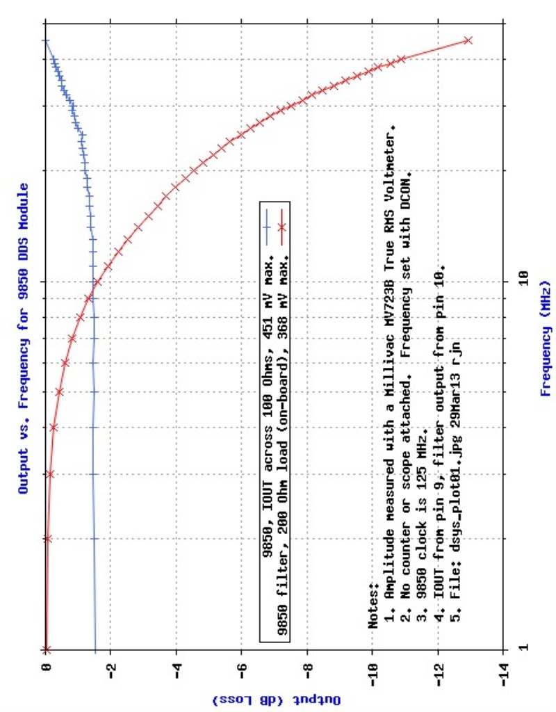
Figure 7 -- DDS Output vs. Frequency
Page 34
(BLANK)
Page 35
Commands are provided to set the phase value in the DDS modules but there are some limitations and caveats, as noted below.
To specify a phase value, first enter it into the holding register. Use the "p" and "P" commands to write the phase value into the DDS A and DDS B phase bytes, respectively.
The phase value loaded into the holding register should be in the range of 0 to 31 ($00 to $1f). Numbers larger than this are clipped to a maximum of 31 and sent to the aphase and bphase registers without further validation. The phase values for the frequency registers are shown with the information command as a "p" character followed by a two-digit hexadecimal number. These phase values are shown just after the frequency registers.
The phasing commands were observed to work without obvious errors at frequencies up to 15 megahertz, but slight phase discrepancies were noted at higher frequencies. These discrepancies were relatively small and may have been caused by our test setup or by the DDS filter network. The cause of the discrepancies was not investigated and users are cautioned to determine the phasing performance and the suitability of DDS modules before incorporating them into an application.
To observe the action of the phasing commands, we suggest using a frequency of a few megahertz. Note: the same clock must be used for both modules. Set the oscilloscope to trigger on the DDS with a phase of zero (e.g., DDS A). Phase shifts can be observed on the second DDS (e.g., DDS B) as its phase value is changed. We suggest using the "z" command when sending a new phase difference to both DDS modules, although the "a", "A", "b" and "B" commands also ensure proper phase synchronization.
The requirements for accurate phasing two DDS chips is described in the Analog Devices Application Note AN-587. The note recommends a number of hardware modifications that may be required to provide accurate phasing for critical applications. Although our test modules, operated with a common clock, have exhibited the expected response to phasing commands, we recommend reading the the application note before employing DDS modules in your application. Some of the recommended measures are difficult to implement with the off-the-shelf DDS modules for which DCON is intended. Here are some considerations:
In summary, using a common clock source for both modules, the DCON controller can control the phasing of two DDS modules. Although the results are acceptable for most applications, phased modules should be verified in the application of interest.
Page 36
Notwithstanding the cautions given above, the phased operation of two DDS modules can provide satisfactory results in many applications over a wide frequency range. For example, Figure 8 shows quadrature DDS outputs at 10 Megahertz. These were obtained by leaving the DDS B phase at zero and setting the DDS A phase to "8", resulting in a relative phase difference of (8 steps)(11.25 degrees/step ) = 90 degrees.
One way to observe how accurately the signals are phased is to set their amplitudes equal to each other (e.g., with an attenuator on one channel) and set the phase difference to 180 degrees (e.g., p=16, P=0). With these settings, observe the "A+B" output on an oscilloscope: it should show that the two signals exactly cancel.
Refer to the ELITE project documentation to see how to build an audio or RF phase meter.
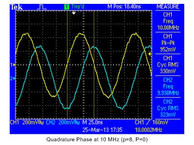
Figure 8 -- Quadrature Outputs at 10 MHz
Page 37
The scale factor settings for the A and B clock frequencies are stored in the "ascale" (ascale) and "bscale" (bscale) registers. To display these registers, use the "i" or "I" commands.
At startup, with default values, the scaling registers both contain a rather cryptic 32-bit hexadecimal number, $225c17d0. This is the value used to calculate a DDS load value based on the default clock frequency of 125 MHz. This is the most common clock frequency used by 9850 DDS modules. The controller can operate with several different clock frequencies. The operating frequencies for DDS A and DDS B can be different.
Clock frequency settings are entered with commands that begin with an "x", followed by the frequency in megahertz. For example, to configure DDS A or DDS B for operation at 100 MHz, first enter the "x100" command.
The "x" commands load the new scaling factor into the holding register. After entering a new clock frequency, use the "i" command to verify the new content of the holding register. To update the scaling factors for DDS A or DDS B, use the "s" and "S" commands, respectively.
After loading a new scaling factor into the A or B scaling registers, any new frequencies entered are calculated with the new scaling factor. Because afreq and bfreq are calculated with the current scaling factor, the frequency registers contain the old frequency values until new frequencies are entered.
For example, to change DDS A for operation at 100 MHz, enter the "x100" command followed by the "s" command. Because the frequency register contains a value that was calculated with the previous clock setting, the frequency must be re-entered. For example, to re-establish a frequency register setting for 1000 Hertz, enter "#1000" followed by the "A" command. After changing the clock frequency and re-entering the startup frequencies, executing the "!" command ensures that the processor starts up with the new scaling factor and the revised startup frequencies.
Because the controller also supports 9851 DDS modules, there is a "x180" command to support a 9851 operating at 180 MHz (i.e., a 30 MHz crystal and a multiplier of 6). To configure DDS A or DDS B for operation with a 9851 operating at 180 MHz, enter the "x180" command followed by the "s" or "S" command, as appropriate.
The controller must be set for operation with either the 9850 or 9851 chips for the scaling commands to operate correctly.
For example, to use a to use a 9851 operating with a 180 MHz clock on DDS B, use the "x180" and "S" commands followed by the "/51" command.
Page 38
The clock scaling commands given above may have to be changed for modules operating at other clock frequencies or for a clock frequency that is not exactly equal to 25 MHz, 50 MHz, 100 MHz, 125 MHz or 180 MHz. Fortunately, it is possible to adjust for different clock frequencies by loading custom scaling factors. This can be done for most clock frequencies by calculating the required scaling factor and loading it into a scaling register. This requires a bit of math but the procedure is straightforward, as outlined below.
The 9850 datasheet provides an equation for calculating a frequency based on the clock frequency and the 32-bit value loaded into the 9850 chip's frequency register. To calculate a custom scaling factor, a value must be calculated that corresponds to the number of counts needed to change the output frequency by one Hertz. This "counts per Hertz" value is the reciprocal of "delta" in the datasheet equation. The "counts per Hertz", CPH, can be calculated for a new clock frequency, as illistrated in the following:
	CPH (Counts per Hertz) = (2exp32)/(clock)

	CPH ( 25 MHz) = (2exp32)/(25,000,000 Hertz)  = 171.79869184  counts/Hertz
	CPH ( 50 MHz) = (2exp32)/(50,000,000 Hertz)  =  85.89934592  counts/Hertz
	CPH (100 MHz) = (2exp32)/(100,000,000 Hertz) =  42.949672960 counts/Hertz
	CPH (125 MHz) = (2exp32)/(125,000,000 Hertz) =  34.359738368 counts/Hertz
        CPH (180 MHz) = (2exp32)/(180,000,000 Hertz) =  23.860929422 counts/Hertz
The CPH result for 125 MHz means that, for every one-Hertz increase in output frequency, approximately 34 counts must be added to the current frequency value. If the controller could easily handle fractional numbers, this value could be used directly to calculate the DDS load value.
For example, multiplying CPH times the desired frequency and converting the result to the nearest hexadecimal value gives the value to load into the DDS frequency register. Doing this for a frequency of 1,000 Hertz results in a load value of $8637, the default value for the afreq and bfreq registers.
Page 39
The controller performs calculations with scaled integer arithmetic. Scaling is needed to account for the fractional part of the CPH value. Ignoring the fractional part accumulates very large errors in the load value.
To provide a high accuracy, the controller applies the scaling factor of 2exp24 (two to the 24th power) to the CPH factor. To enter the 2exp24 scaling factor on the Windows scientific calculator, "Calculator", press 2, followed by the "x^y" key, followed by an entry of 24. Multiplying this number by the CPH factor for 125 MHz yields a result that, when converted to Hexadecimal, is $225c17d0, the default scaling factor loaded into ascale and bscale.
Here are the pre-calculated scaling factors used by the controller:
	Scaling Factor = (CPH)(2exp24) = (CPH)(16,777,216)

         25 MHz scale factor = (171.79869184  counts/Hertz) (2exp24) = $abcc7711
 	 50 MHz scale factor = ( 34.359738368 counts/Hertz) (2exp24) = $55e63b88
	100 MHz scale factor = ( 42.949672960 counts/Hertz) (2exp24) = $2af31dc4
	125 MHz scale factor = ( 34.359738368 counts/Hertz) (2exp24) = $225c17d0
        180 MHz scale factor = ( 23.860929422 counts/Hertz) (2exp24) = $17dc65de
Use the above examples as a guide to calculating a custom scale factor for a new clock frequency. To load the custom value into ascale or bscale, first enter it (in hexadecimal) into the holding register. Use the "i" command to examine the holding register to verify correct entry.
Once the scale factor is verified, use the "s" command to transfer the value to the scaling register for DDS A. Use the "S" command to load the scale factor into the scaling register for DDS B.
There is no need to re-enter the scaling factor if you want to set both DDS modules to the same value: just enter the scaling factor followed by the "s" and "S" commands. Because scaling is changed infrequently, there is no single command to set both DDS modules to the same scaling factor.
Note: after entering a new scaling factor, the frequency registers must be re-loaded to apply the new scaling factor to the frequency registers.
Because the scaling factor for clock frequencies under 17 MHz requires a 5-digit scaling factor, the controller does not support custom clock frequencies below 17 MHz.
One common use for a custom scaling factor is adjusting for the DDS module's clock frequency. Directly measuring the DDS clock frequency at the on-board oscillator terminal is not recommended because of errors due to factors such as probe loading.
We recommend that you estimate the clock frequency using a frequency setting that will be off by a known amount. For example, with a 125 MHz nominal clock frequency, the DDS can be set to 12.5 MHz and the clock error estimated as one-tenth of the actual output frequency error.
Page 40
The CPH value can be used to estimate the number of counts to add or subtract from the nominal scaling factor. This process can be repeated, as needed, to obtain the desired accuracy.
The following shows how to adjust the clock frequency scaling factor for a DDS clock that is not exactly 125 MHz. This example is based on an actual adjustment session in our lab.
Setting the DDS frequency to 12.5 MHz and observing the actual output frequency, the measured frequency was 20 Hertz high. To correct for this, the scaling factor needed to be adjusted lower from the default of $225c17d0. Because the clock was off by 20 Hertz at 12.5 MHz, it was estimated that the clock at 125 MHz was high by approximately ten times this amount, 200 Hertz.
Here is the procedure we used to set a new scaling factor:
    1. Calculate the new estimated scaling factor from the estimated clock frequency:

	           CPH = (2exp32)/(125,000,200 Hertz) = 34.359683392... counts/Hertz
	scaling factor = (2exp24)(34.359683392 counts/Hertz)
                       = 576,459,829.967695539... =~ $225c1435

    2. Load the approximate scaling factor and reset the frequency to 12.5 MHz:

        0>$225c1435
	0>s
        0>#12500000
        0>A

    3. The resulting frequency is 12,500,004 Hertz, still too high.
       This is primarily a result of rounding errors (e.g., decimal to hex conversion).

    4. Re-calculate using the new estimated frequency:

	CPH = (2exp32)/(125,000,240 Hertz) = 34.359672397... counts/Hertz
	scaling factor = (2exp24)(34.359672397...)
                       = 576,459,645.500904126... =~ $225c137d

    5. Load the new estimate of the scaling factor and reset the frequency to 12.5 MHz:

        0>$225c137d
	0>s
        0>#12500000
	0>A

    6. The frequency is still too high by about 2 Hertz.
       Adjust the frequency down a bit more:

	(2 Hertz)(34.359683392... counts/Hertz) = 68.719344794... =~ $44 counts
        $225c137d - $44 = $225c1339

    7. After loading the new scaling estimate, the frequency error was very small.

    8. Save the scaling factor using the "!" command so that it is restored at startup.
Page 41
We have run two side-by-side modules from a single clock by removing one crystal and wiring a short one-inch jumper between the modules. This modification was performed to allow common scaling factors for the two modules. This modification is shown in Figure 4, an overview photo of Development System 1. Although the short jumpers worked for the Figure 4 configuration, longer two inch jumpers on a second development board did not work. Also, removal of the factory oscillator cans was somewhat difficult.
Figure 5 shows a closeup of the Development System 1 board with two DDS modules driven with a can-type crystal oscillator mounted on the main circuit board. This is the configuration used to verify operation at different frequencies. The photo shows the board configured for operation at 50 MHz. This scheme seems to work better than the jumper scheme shown in Figure 4, provided that the leads from the clock output to the DDS modules are short and of equal length. We also used single-point grounding for the modules and the crystal. Note that the crystal and modules are located close to the 5 Volt power entry point.
Although these single-clock wiring schemes worked for our particular hardware configuration and wiring, we cannot recommend or support such modifications.
The lower clock frequency limit of 17 MHz prohibits the direct use of the controller with the 10 MHz output of rubidium reference sources. Some of the references have the ability to generate output frequencies higher than 10 MHz -- these can often be used directly with DDS modules by removing the on-board oscillator can and feeding the multiplied output directly to the pad connected to the DDS clock input.
Users with a rubidium reference with only a 10 MHz output can use a Phase Locked Loop (PLL) to multiply the 10 MHz signal to a frequency compatible with the controller. For example, we have used our own PLL module, DECL, to multiply the output of a rubidium reference to 50 MHz, feeding the output to two DDS modules. This scheme worked for us, but we cannot support custom hardware modifications and configurations.
Users interested in an easy interface to some commonly-available rubidium sources may want to look at our FEBO product at the Kibler Electronics site. This site also describes the DECL product.
Page 42
The DDS modules can be turned off either individually or a at the same time. To stop the output of DDS A, use the "x" command. To stop the output of DDS B, use the "X" command. To stop both outputs, use the "xx" command. To restart the outputs using the contents of the afreq and bfreq registers, use the "a", "b" or "z" commands. Any one of these commands will restart both DDS outputs.
The DDS modules can be individually powered down. In the power down mode, a DDS draws much less power than when it is active. The 9850 datasheet gives a typical operating dissipation of 380 milliwatts for operation at 5 Volts with a 125 MHz clock. When powered down, under the same operating conditions, the chip typically dissipates only 30 milliwatts.
Before powering down a module, first turn its output off using the "x", "X" or "xx" commands. To power down DDS A, use the "d" command. To power down DDS B, use the "D" command. To power the chips back up, use the "u" and "U" commands, respectively.
Note: once the DDS modules are powered back up, the outputs are not automatically restored. To turn the outputs back on, use the "a", "b" or "z" commands. Any one of these commands will restart both DDS outputs.
Use the "r" (reset) command to reset the controller and both DDS modules. Because the reset line is wired to the reset line on both modules, the modules cannot be individually reset. The "r" command jumps to the controller's cold start routine that, in order, performs the following:
Page 43
The controller output levels can be set to either open drain or push-pull. The default configuration is push-pull. With a push-pull configuration, the DDS module inputs are driven at the controller logic levels, 3.3 Volts. Normally, this logic level is adequate even for DDS modules operated at 5 Volts. We have tested a number of modules and have not found any that did not operate at logic levels of 3.3 Volts.
However, the 9850 datasheet specifies a minimum logic level of 3.5 Volts for a chip operating with a 5 Volt supply. To ensure that the DDS module inputs operate at 5 Volt levels, the controller outputs can be configured as open drain and pulled up to 5 Volts through a pullup resistor. When configured for open-drain operation, the controller output must must be pulled up to the 5 Volt supply. Figure 1 shows the wiring of these pullups.
To configure for pullups and open drain operation, use the "/od" (init open-drain) command. To reconfigure for push-pull outputs, use the "/pp" (init push-pull) command. Normally, with controller outputs wired to 5 Volts through pullups, the open-drain configuration should be saved to flash, as described below.
To restore the factory defaults use the "//" command. Note that this restores only the volatile memory locations, such as afreq and bfreq, and does not affect configuration values stored in flash memory. If you have saved a configuration to flash memory, this will be the configuration restored when DCON is rebooted or when the "/" command is executed.
If the controller configuration has been saved to flash memory, this configuration is restored from flash memory at startup. To save the current configuration to flash memory, use the "!" command. Use the "!!" to command all units connected to a serial input. This stores their configurations to flash. To restore a configuration from flash, use the "/" command..
The default configuration can be restored. To restore the defaults to the flash memory, first execute the "//" command followed by the "!" or "!!" commands.
Configuration changes are not automatically saved to flash for several reasons. First, execution of command combinations, as needed, provide more flexibility in managing the controller's configuration. Also, there are limits on the number of flash writes are possible before flash errors occur.
The Silicon Laboratories dataheet for the C8051F300 chip gives the guaranteed number of read/write cycles as 20,000. This is very conservative with typical values in the hundreds of thousands. Silicon Laboratories notes that their tests show improvement in flash write limits when flash is erased twice before writing. The controller erases flash memory twice to potentially improve the flash write limit. It is unlikely that the controller's flash write limit will be exceeded in normal operation.
Page 44
Use the "v" command to send the current version to the serial port. The version consists of the application name (e.g., DCON) followed by the device address and the date of the last firmware compilation in "YYMMDD" format. For example, the version string "DCON 01 120923" represents a device address of 1 and a compilation date of September 23rd, 2012.
To query the controller for its port assignments, use the "q" command. This is the output of this command:
	P0.0=ERROR P0.1=FQ_UD P0.2=DATA  P0.3=W_CLK_A
	P0.4=TX    P0.5=RX    P0.6=RESET P0.7=W_CLK_B
The output shows only how the logical port bits are assigned to the DDS signal lines. Refer to Figure 1 for the physical pin assignments relative to the port and signal assignments.
For controllers commanded by a processor and not by a person sitting at a terminal, it is useful to disable all serial responses to improve processor response time. To disable serial responses, use the "N" command. To enable serial responses, use the "n" command. The default is to enable all serial responses.
Note that, although the "N" mode does improve responsiveness, command execution time can be unpredictable (e.g., during calculation of a new frequency load value). Thus, care must be taken when sending a command and relying on a fixed time for it to complete.
To avoid having to allow a fixed time for command completion, the "N" command also changes the behavior of the error output. Normally, the error output goes low (turns on the error LED) to indicate an error. When serial responses are disabled, the error output goes low to indicate either a command error or a command completion.
When a new command is started, the error output is set high. It is set low again either on a command error or command completion. Thus, the error output indicates command completion, errored or not. After sending a command, a command processor can monitor the error output to detect when the next command can be sent (i.e., when the error output goes low).
There is one small caveat: in the case of an error, there is a slight delay between the error output going low and the interpreter's readiness to accept a new command. To guard against this case, there should be a fixed delay of approximately three microseconds, after the error output goes low, before sending a new command.
Page 45
The default setting for all controllers is to always execute all commands. For those few applications that require serial control of more than two DDS modules, an address can be assigned to each controller. Up to 256 addresses can be assigned.
Controllers with an address can be set to listen for commands or to ignore commands. Commands are also available to set all controllers to listen or to ignore status. This global addressing can be reset with all addresses reverting to their listen/ignore status prior to the execution of the global commands.
Following sections describe how to use the addressing commands and how to manage serial responses and error indication from multiple controllers. These sections also provide recommendations and examples to help explain some ways that addressing can be used to manage a multi-controller environment.
Use the "i" command to observe the address currently assigned to a module. The module address is also shown by the "v" (version) command. The address is displayed in the information report as a hexadecimal value following the "adr:" label. The default value for the address is $ff.
Before assigning an address, ensure that the controller being set is only module listening on the serial link (i.e., disconnect all but the module being set). To assign an address to a module, first enter the address, in the range of 0 to 255 ($00 to $ff), into the holding register. Use the "L" command to save the holding register in a temporary register. This register is used to set the controller's address when the controller's configuration is next saved to flash memory.
Save the address to flash with the "!" command after ensuring that all other startup settings are correct (e.g., afreq and bfreq). After an address is assigned and saved to non-volatile memory, the module can be used in a multi-controller (multi-drop) configuration.
Page 46
To set a controller to listen for commands, first enter the listen address in the holding register. Once the holding register is set with the listen address, use the "l" command to configure a controller to listen on the serial link. The "l" command always executes at all addresses.
To ensure that only the addressed unit sets itself to a "listen" status (listen), all units check to see if they are the unit being addressed. To do this, they get their assigned address from flash and compare it with the value in the holding register. If these two addresses match, the controller is set to listen.
To set a controller to ignore commands sent to its address, first enter the address in the holding register. Once the holding register is set with the address, use the "k" (kill) command to set the addressed controller to an "ignore" status (ignore). The "k" command always executes at all addresses. Kill address checking is the same as for the listen command.
Page 47
To address groups of controllers, set all of the controllers in the group to listen and kill all other addresses.
For example, assume that there are three units being addressed, one with an address of $01, one with an address of $02 and one with an address of $03. To set controllers 1 and 2 to listen and to set controller 3 to ignore commands, first enter $01 in the holding register, followed by the "l" command. Next, enter $02 in the holding register, followed by the "l" command. Finally, enter $03 in the holding register, followed by the "k" command.
Note that holding register entries and the "l" and "k" commands always execute at all addresses. There is no need to globally enable all addresses before entering a value or issuing the "l" and "k" commands.
To address all units regardless of their listen status, use the "g" (global) command. This command temporarily sets all units to listen status. Use the "G" command to restore the listen/ignore status for all controllers.
In some cases, it may be easier to form a group by disabling all units and then setting some of them back to the "listen" status. To kill all controller addresses, use the "m" (mask) command. As with the "g" command, the "m" command saves the current status of each controller so that it can be restored. As with the "g" command, use the "G" command to restore the previous listen or ignore settings for all controllers.
Note that the "l" and "k" commands also save their listen/restore status as the restoration status. This prevents an unexpected change in status if listen and kill commands are executed after a "g" or "m" command and before a "G" command.
Serial responses from multiple modules can be handled in a number of ways. If only errors are to be monitored, the serial response lines can be left unconnected and the error indicator pin for each module can be monitored for errors. For microprocessor control, this requires an input pin for each module. If necessary, logic chips can be used to "or" multiple error outputs to provide a general error indication. Typically, a control microprocessor knows the last unit addressed and can monitor the "ored" error indicator for an error.
Monitoring serial responses from multiple modules is more problematic. The serial logic-level outputs of multiple modules can be "ored" together with logic chips and the addressing capability of the controller can be used to set only one module at a time to respond. This "poll for status" approach is a bit cumbersome but adequate for all but the most demanding applications. Another approach is to multiplex responses with logic chips and use external hardware addressing (e.g., with spare digital outputs from a control microprocessor).
Page 48
For configurations with only a single controller and DDS module, the output used for clocking data into DDS B, shown as W_CLK_B on the schematic, can be used as general purpose output. Typically, this applies to a controller attached to a single DDS with the unused clock line used to control another device (e.g., a Push To Talk relay for Amateur Radio applications).
To see output pin mapping, refer to Figure 1.
To set port 0, bit 7 (P0.7), use the "O" command; to clear P0.7, use the "o" command. Note that P0.7 appears on the DCON's P1 connector, pin 2.
To toggle port 0, bit 7 (P0.7), use the "t" command.
If necessary, this pin can be configured as open drain or push-pull with the "/od" and "/pp" commands, respectively.
Page 49
![]()
An on-board 3.3 Volt regulator provides stable regulated power to the Module. It operates with power inputs from 5 to 16 Volts. To configure the module for operation, connect either or both of the "GD" (ground) pins to the return of the supply (ground) and connect the "+5" pin to the input voltage (e.g., 5 Volts).
The module operates with power inputs from 5 to 16 Volts.
Although voltages higher than 5 Volts can be applied to the "+5" pin, the label was selected for compatibility with the Test/Programmer Board which operates at a supply voltage of 5 Volts.
Once the input voltage is applied between the "+5" and "GD" pins, the operation of the regulator can be verified by measuring the voltage between the GD (ground) and the "VD" pin. The regulator output voltage should be close to 3.3 Volts. If you plan to operate the module directly from an off-board supply, remove the regulator chip and install a jumper between the input and output pads. This, for example, could be used for a module operating on a 3 Volt battery.
Page 50
The controller chip's quiescent current draw will vary but is approximately 10 milliamperes at the processor's internal clock rate of 24.5 MHz. The maximum regulator output is 100 milliamperes.
Although the maximum current for the chip outputs is 500 milliamperes (total), with all outputs heavily loaded, this is not possible with the 78L33 regulator. If the application requires currents higher than the 100 mA maximum of the regulator, an external regulator or high-current voltage source (e.g., a battery) must be used. To use an external regulator, remove the regulator chip and solder a wire across the regulator input and output pins before applying the externally-regulated power between the "+5" pin and either or both of the "GD" (ground) pins.
The chip digital outputs, when configured for push-pull operation, are rated for a maximum current of 100 milliamperes each with a maximum total chip current (including quiescent current draw) of 500 milliamperes. Chip outputs are 5 Volt tolerant.
Be aware that the total regulator dissipation is 250 milliwatts and the maximum regulator output is 100 milliamperes. We recommend that the dissipation be kept below half the dissipation limit and below the maximum current limit. The regulator is both current and temperature limited in the event of output overload.
Page 51
| a (output afreq) | Set the output of DDS A from afreq, the frequency register for DDS A (same as the "b" and "z" commands) |
| A (set/out afreq) | Set the output of DDS A from the holding register & write holding register to the A frequency register. |
| x25, x50, x100, x125, x180 | Load the scaling factor for various clock frequencies into the holding register (e.g., 100x for a 100 MHz clock). Use the "s" and "S" commands to set the frequency registers from the holding regulator. |
| b (output bfreq) | Set the output of DDS B from bfreq, the frequency register for DDS B (same as the "a" and "z" commands). |
| B (set/out bfreq) | Set the output of DDS B from the holding register & write the holding register to the frequency register for DDS B. |
| c (clear) | Clear an error condition, setting the error pin, P0.0, high and clearing the error counter. |
| d (A down) | Power down DDS A |
| D (B down) | Power down DDS B |
| e (error) | Force an error, pulling the error pin, P0.0, low and incrementing the error count. |
| f | Decrement (fudge) the afreq frequency register downward by the amount specified by the holding register. Also see the "j" command. The decremented frequency takes effect when the "a" command is executed. |
| F | Decrement (fudge) the bfreq frequency register downward by the amount specified by the holding register. Also see the "J" command. The decremented frequency takes effect when the "b" command is executed. |
| g (global) | Set address mask to $ff so that commands are executed by all devices. The previous command mask is saved at each drop so that it can be restored with the "G" command. |
| G (restore global) | Restore the address mask to its value prior to execution of the global (g) command. |
Page 52
| Command | Description |
| h (set A from hold) | Output the holding register to DDS A without affecting afreq, the frequency register for DDS A. Values can be specified in decimal (a frequency) or hexadecimal (a DDS load value). Output is from the temp register: the holding register entry is not affected. |
| H (set B from hold) | Output the Holding Register to DDS B without affecting bfreq, the frequency register for DDS B. Values can be specified in decimal (a frequency) or hexadecimal (a DDS load value). Output is from the temp register: the holding register entry is not affected. |
| i (info) | Send chip register information to the serial port |
| I (extended info) | Send extended chip register information to the serial port |
| j (A adjust) | Adjust frequency register for DDS A (afreq) upward. The amount to increment the frequency is specified by the holding register. There is no command to adjust frequency downward. |
| J (B adjust) | Adjust frequency register for DDS B (bfreq) upward. The amount to increment the frequency is specified by the holding register. |
| k (kill) | Disable (kill) the address in the hold register. Also save the kill status as the "restoration" status for the "G" command. |
| l (listen) | Enable (listen) address in the holding register -- effective only if the address in the holding register and the address stored in flash are the same (i.e., only applies to the device addressed). Also save the listen status as the "restoration" status for the "G" command. |
| L (listen address) | Set the device address from the holding register -- all other devices on the serial bus must be disconnected! To save address to flash, execute "!!" command after all other registers are set to their startup values. |
| m (mask) | Disable (kill) all controllers, saving their current listen/ignore status. Restore the current status with the "G" command. |
| n | Respond normally to keyboard input (echo back, prompting) |
| N | Disable serial responses -- in this mode, the error output, P1/5, indicates either an error or command completion (low true). |
| o | Clear P0.7 -- for configurations not requiring a second DDS, this can be used as a general purpose output (e.g., driving a PTT line for Amateur Radio applications. |
| O | Set P0.7-- for configurations not requiring a second DDS, this can be used as a general purpose output (e.g., driving a PTT line for Amateur Radio applications. |
| p | Set phase value (0-16) for DDS A from the holding register |
| P | Set phase value (0-16) for DDS B from the holding register |
Page 53
| Command | |
| /od (set open drain) | Configure output pins for open drain operation. Use this command for DDS module inputs that must be pulled up to 5 Volt logic levels. Most DDS modules do not need to be pulled up. |
| /pp (set push-pull) | Configure output pins for push-pull (default). DDS inputs will operate at the 3.3 Volt supply voltage. |
| q (query) | Display port/signal assignments. |
| r (reset) | Reset the controller and both DDS chips. |
| s (set A scale) | Load a hexadecimal scale value for DDS A from the holding register -- use "$" for hex entry |
| S (set B scale) | Load a hexadecimal scale value for DDS B from the holding register -- use "$" for hex entry |
| t (toggle) | toggle P0.7 -- for configurations not requiring a second DDS, this can be used as a general purpose output (e.g., driving a PTT line for Amateur Radio applications. |
| u (A power up) | Power up DDS A |
| U (B power up) | Power up DDS B |
| v (version) | Display the application name and version date in YYMMDD format. |
| x (A off) | Stop DDS A output |
| X (B off) | Stop DDS B output |
| xx (dos equis) | Stop both the A and B DDS outputs |
| y | Set the afreq frequency register from the holding register without affecting the output frequency. Use the "a" command to make the change take effect. |
| Y | Set the bfreq frequency register from the holding register without affecting the output frequency. Use the "b" command to make the change take effect. |
Page 54
| Command | |
| z (zend A & B) | Simultaneously update the outputs of both DDS modules. Both the afreq and bfreq register contents are sent to both DDS modules. |
| za (zend A to both) | Simultaneously update the outputs of both DDS modules using the afreq register contents. Restore previous outputs with the "z" command. Note that the A and B DDS frequencies will be the same only if their clock frequencies and scaling factors are the same! |
| zb (zend B to both) | Simultaneously update the outputs of both DDS modules using the bfreq register contents. Restore previous outputs with the "z" command. Note that the A and B DDS frequencies will be the same only if their clock frequencies and scaling factors are the same! |
| Z (zend A to both) | Obsolete as of version 130406 (replaced by "za" and "zb"). Formerly used to send the afreq frequency to both DDS A and DDS B. This command does not affect the bfreq frequency register. Note that the A and B DDS frequencies will be the same only if their clock frequencies and scaling factors are the same! |
| /50 (default) | Set both DDS channels to operate with a 9850 chip. |
| /51 | Set both DDS channels to operate with a 9851 chip and a PLL multiplier of 6. |
| / (init) | Restore settings from non-volatile memory (flash) |
| // (init defaults) | Restore settings to default values |
| ! (save to flash) | Command: save settings to flash, Response: processor has rebooted |
| !! (save, global) | Save settings to flash, global addressing |
| # (enter decimal) | Enter a decimal number (e.g., #001234) |
| $ (enter hex) | Enter a hexadecimal number (e.g., $09A4DE) |
Page 55
Figure 4 shows an overview of a Development System. This is one of the systems used to develop the controller firmware and to test production controllers.
Along the top of the figure is the serial connection to the controller board. It uses the FTDI Breakout Board. The breakout board converts USB to logic levels. Attached to the FTDI Breakout Board is an adaptor that converts logic levels to RS-232 levels. The RS-232 signals are routed through gender changers and a crossover adaptor and connected to a second module that converts RS-232 levels back to logic levels for the controller.
This mighty kludge is not normally needed but is just an artifact of an earlier development environment that required RS-232 levels and connectors. The Breakout Board can be directly connected to the controller, similar to the connection shown in Figure 1 for the FTDI Friend module.
Below the serial cabling and to the left side of the photo is a small board assembly used to provide grounding and probe connection points.
At the middle right is the controller development board with two controllers and two side by side DDS modules. Note that one of the DDS modules has a crystal and that the other does not. Also note the small black and yellow wire pair connecting the two modules. This connection ensures that both modules operate from the some clock source. Longer jumpers may not work and this kind of board to board connection is not recommended.
The two controllers have error LEDs connected (one red, one SMT blue). Besides power and an RS-232 input, the only hardware connected to the top controller is the error LED. This module is used to test the addressing commands for a multi-drop configuration. The lower controller module connects to both DDS modules for normal command execution.
Page 56
At the bottom left of the development board are, in sequence, the 5 Volt power connection, a power indicator LED, a can-type crystal oscillator and a 6-pin connection to the FTDI Friend. The Friend module is plugged in to illustrate its connection point but is unplugged during development with the other serial connection. The crystal oscillator is also installed to illustrate its location but is not being actively used in the board configuration shown in Figure 4.
In an alternative test connection, the oscillator connects to two DDS modules with their crystal oscillators removed. The piece of blue tape covers the ends of the wires used to connect the crystal oscillator to the two DDS modules. This configuration is used to test operation with different frequency crystal oscillators (e.g., to verify scaling constants).
The output connection from the DDS modules are near the top left of the board and connect to the grounding/access board with a color-coded cable. Each wire end in the cable has a single socket connection. Two wires it the cable carry the DDS outputs to the grounding/access board where they land on individual rows of stake pins that serve as connection points for the oscilliscope probes.
Three other wires in the cable connect from grounded stake pins on the development board to grounded stake pins on the grounding/access board. This is a rather sloppy output connection for high frequency work, but serves to verify the basic operation of the DDS controller.
At the bottom right of the board are two connectors. The bottom connector is a 10-pin shrouded IDC connector that provides a JTAG connection to the Silicon Labs USB Debug Adapter. The connector just above and perpindicular to the JTAG connector provides a 6-pin connection to the level converter on the tail end of the serial cabling chain. The color-coded ribbon cable between the development board and the serial adapter uses 10-pin sockets with only 6-wires punched down. The connector in the center of the ribbon cable provides wire access points for the ttl-level serial signals going to the development board.
Page 57
Both DCON and DSYS modules are delivered assembled and tested. The DSYS modules are tested with the DDS module and serial adapter supplied with the assembly. The DCON modules are tested with a dual DDS development board, as described below. The following functions are tested (in the order given):
Addressing and open-drain configurations are not tested. The DSYS assemblies are tested with the CP2102 serial adapter shipped with the assembly. The CP2102 and DSYS assembly are delivered wired to the CP2102 with jumper wires for the filtered DDS output. Power for DSYS tests is derived from the CP2102. All DCON testing uses an external 5 Volt wall wart rated at 1 Ampere.
Page 58
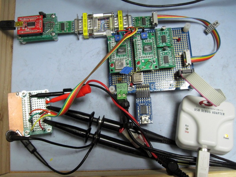
Page 59
Figure 5 shows a closeup of the processor/DDS board for Development System 1.
This cloesup shows the development board layout in more detail, especially the routing of the clock jumper. Note that the board was built with a Parallax prototyping board (cheap, excellent quality).
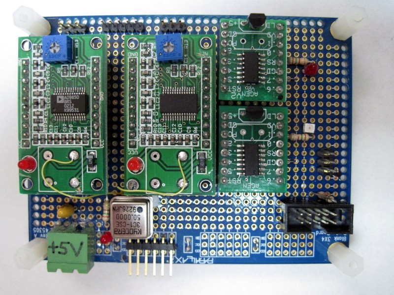
Page 60
(BLANK)
Page 61
Figure 6 shows a second dual-DDS development system using the MUTS programmer in place of the DCON Module. This was done with this earlier development board to allow the Silicon Laboratories USB Debug Adaptor to remain plugged in during development. It also simplifies RS-232 connection with a standard cable connection. The Debug Adaptor is connected to the 10-pin shrouded connector on the left side of the programmer. The serial interface connects with half of the 10-pin cable on the right of the programmer. The serial pin connections are shown at the top middle of Figure 1 (PL3).
To provide access to the bottom of the MUTS programmer board, it is raised up from its motherboard with small standoffs. Wires soldered to the Module's socket pins on the bottom of the programming board connect to the DDS Modules.
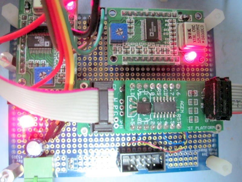
Page 62
If you have just received your DDS controller, you probably want to get it going quickly without wading through all of the documention. This section describes how to quickly set up the controller and verify its operation.
Figure 1 shows how to interconnect the controller to an RS-232 converter and to two DDS modules. We suggest hooking up just one DDS to start.
To hook up single DDS, ignore the wiring to DDS B. The wiring shown for the RS-232 adaptor and the DDS modules is based on the most popular products that we have found on EBay. You may want to plug the controller and the DDS module(s) into a solderless breadboard or mount the units in sockets soldered to a perfboard (see Figure 4).
For easier reference, you can download controller schematics as a zip file.
Connect positive 5 Volts to pin 9 of the module. This is labeled "+5" on the module. Positive 5 Volts is also needed for the RS-232 adaptor and for the DDS. Check the wiring diagram for the adaptor and module you have to ensure power is applied to the correct pins.
For the controller module, connect the supply "ground" to P1, pin 3 (P1/3) and/or P2/7. We recommend connecting both ground pins. These pins are are labeled "GD" on the PC board (PCB). Also wire and check the ground connections for the DDS modules. The ground connections to D3, D4, D5 and D6 of the DDS are not strictly necessary but are recommended.
Verify the power connections by removing the chips from their sockets and checking continuity with a multimeter. You can also apply power to the sockets and verify the the correct voltages appear at all module pins.
The input signals to the DDS may require pull up resistors, as shown in the schematic. We have found that, although the manufacturer specifies a minimum of 3.5 Volts for the DDS logic pins, the DDS usually operates with the default 3.3 Volt outputs from controller. For a quick start, we suggest leaving out the pull up resistors, installing them only if the DDS module does not work correctly. If the pullup resistors are used, you must set the controller outputs to open drain with the "/od" command (see the Command Summary Table).
Page 63
Connect a serial terminal program to the RS-232 adaptor. Set the terminal for a rate of 9600 baud with 8 data bits, no parity and 1 stop bit. Turn off the "local echo" feature of the terminal program -- the controller echos all commands. If you are using a USB to serial adapter, you may have to check the COM assignment with the Device Manager. You may find that the serial adapter has been assigned an unexpected COM port (e.g., ours was 14).
To perform a quick operational check on the terminal and the computer's serial interface, disconnect the serial adaptor and short pins 2 and 3 of the DB9 connector from the computer. It may be necessary to use a plug to socket adaptor to convert the typical plug output from the computer to a DB9 socket connection that can be easily shorted.
Using a DB9 socket, a heavy duty paperclip can be used for the shorting jumper: it is just about the right size to loosely fit in socket connector pins. With the transmit and receive outputs of the serial connector "wrapped" this way, characters typed on the terminal should be echoed back to the terminal.
Page 64
After reconnecting the serial connection, the DDS and serial interface can be powered up. The DDS modules typically have an LED on the board to indicate that they are powered up. If LED on the DDS module doesn't light, immediately power down the board an re-check the power wiring. To check the controller, feel the regulator to see if it is running hot (it shouldn't be) and measure the 3.3 Volt output of the on-board regulator at pin 7 (P1/7). If 3.3 Volts doesn't appear at pin 7, immediately power down an re-check the wiring to the controller module (or its socket). When checking module power, also check pin 9 (P2/8) to verify the 5 Volt connection.
If power up goes well, verify controller operation with the serial terminal. If the controller is operating correctly, it will display a "!" character at power up to signal that it has rebooted. Pressing the "Enter" key or space bar gives a response of "0>" to indicate normal operation with no errors.
Enter a "v" to display the application name (DCON), the controller address (default is $ff) and the version date in "YYMMDD" format. Because "v" is a valid command, the controller will respond with a "0>" prompt on the next line after the version. If these inputs or responses are garbled or not present, re-check the baud rate setting on the terminal program or re-check the serial connections (e.g., th RS-232 converter may require a crossover cable). To help troubleshoot the serial connecton, Figure 1 shows data directions -- activity and levels can be verified with an oscilloscope and LEDs on the USB to serial adaptors.
If an error LED is attached to P0.0 output, as shown in the schematic, entering an "e" command lights the error LED. This command forces this pin low to light the LED. The error forced by the "e" command can be cleared with a "c" command -- this will also turn off the error LED. Note that command errors are indicated with a "?" response and a prompt that shows a non-zero error count. For example, the "0>" in the prompt changes to "1>" if there is a single error. As noted above, when the module powers up or reboot (e.g., in response to a "r" command), the prompt is an exclmation point (!).
If the controller module appears to operate correctly, enter an "i" command -- this displays a report showing the contents of the controller registers. The registers should be loaded with defaults that produce a 1000 Hertz output. With an oscilloscope connected to the output of DDS A (e.g., at the "ZOUT" pin), a 1000 Hertz sine wave should appear at the DDS output. If this output isn't exactly 1000 Hertz, do not be concerned: this may be because the default setup assumes your DDS module is operating at a clock rate of 125 MHz. Also, if the clock is not exactly 125 MHz, the frequency may be slightly off. This can be corrected as described in other sections in this manual (e.g., see the "s" and "S" commands in the Command Summary Table.
If a second DDS is connected, a 1000 Hertz sine wave also appears on the DDS B output at startup. These outputs can both be turned off by entering the "xx" command. To turn them both back on again, use the "z" command.
The above checks basic functionality. There are a number of other commands to control the DDS modules. Refer to the Command Summary Table for a synopsis of the controller commands. Each of the commands in the table are linked to the sections of this manual that describe their operation in more detail.
Page 65
The following parts list is for the AGEN Module populated with only the reset and regulator components for use with the DCON Serial DDS Controller Module.
| Part | |||||
| R3, R6, R7 & R13 | RES, 1K, 1/8W, 1%, 0805 | Digikey | 541-1.00KCCT-ND |
||
| C1 | CAP, 10uF, 10V, X5R, 0805 | Digikey | 490-1709-1-ND |
||
| C2, C9 | CAP, ceramic, 1uF, 25V, Y5V, 0805 | Digikey | C2012Y5V1E105Z/0.85 |
||
| C10 | CAP, 0.1uF/25V, 10%, 1206 | Stock | N/A |
||
| U1 | REG, 3.3 Volt, TO-92, 100 mA, 250 mW | Digikey | 497-7288-ND |
||
| U2 | IC, C8051F300GS microprocessor, pre-programmed | Digikey | 336-1535-5-ND |
||
| PCB | PCB, AGEN | ||||
| P1, P2 | HDR, 17-pin header, SIL, breakaway | FRYS | PLS-40S-P5 |
Page 66
Original circuit, Rev. B of the schematic |
||
Revision 1 of the documentation. |
||
Revision 2 of the documentation. Everything is now Figures vs. Photos, Schematics, Figures, etc. Also, schematics and photos are now placed in the text body instead of links to local files (for PDF conversion, etc.) |
||
Complete revision for DCON, removing text and features that apply only to the SERF module (not a production product) |
||
Final revision for production. |
||
Revised phasing section. Eliminated reference to obsolete commands (dd and uu). |
||
Revised for vew commands za and zb vs. old Z command that only sent output based on the afreq register. Added testing section. |