Page 2
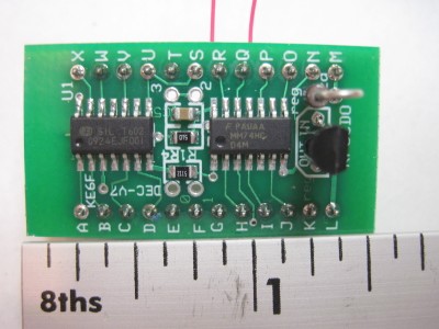
The following describes the design, construction, operation and use of the DECUS divider module. Photo 2 shows a top view of the module and Photo 3 shows the bottom. The primary use of the module is to condition the 10 megahertz (MHz) signal from a rubidium oscillator such as the LPRO-101 or FRS-C units manufactured by EFRATOM Ball, Inc. The DECUS module divides the 10 MHz output from these units to produce marker signals at various frequencies.
The DECUS module also provides buffered 10 MHz outputs that can be used to distribute the conditoned signal to test equipment.
If you require a multiplied frequency output in addition to the decade divisor, you may be interested in the DECL module. If you have a FE-5680 rubidium reference, you may be interested in the FEBO module.
The module's conditioning circuit and divider chip can also be used for other applications requiring signal conditioning and dividing, but this usage is outside the scope of this document.
Page 3
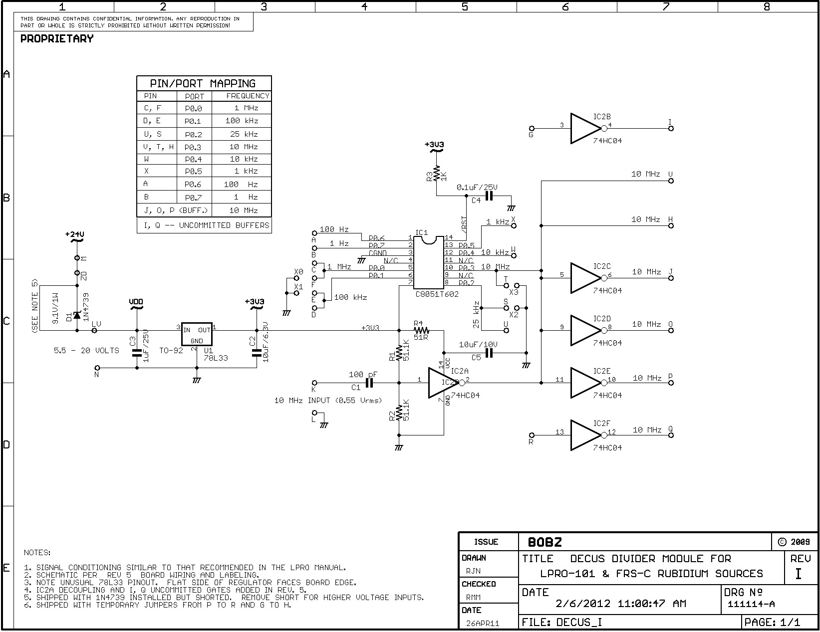
For the following, refer to the DECUS schematic titled "DECUS DIVIDER BOARD FOR LPRO-10 and FRS-C RUBIDIUM SOURCES."
You can download the DECUS schematic as a zip file.
The schematic shows the components, circuitry and some operational restrictions for the module. The Parts List provides additional information about the components used to assemble the module.
As shown in photo 2, the module measures approximately 1 1/4 by 7/8 inches (32 by 23 mm). Signal connections are provided on two 12-pin single row pin headers. The header connections are labeled "A" to "X" for easy reference. Header pins are spaced one tenth of an inch apart and the header rows are spaced 0.6 inch apart. This allows the module to be used with in-line sockets or wired directly to a protoboard.
The module provides nine different divider outputs, ranging from one Hertz to one megahertz. The module also provides three ten megahertz buffered outputs for driving time base inputs of test equipment. Two buffer gates are uncommitted to allow any two of the outputs to be buffered or to allow buffering of an external signal (e.g., a lock indicator for an LPRO or FRS output).
Divider outputs are driven by microprocessor port pins capable of sourcing or sinking up to 100 milliamperes each. The one Hertz output can directly drive an LED to act as an "active" indicator. These drive capabilities are limited by the choice of input voltage and the current limitations of the regulator, as noted in the Power section.
Page 4
The input conditioning circuit is based on the circuit recommended in the LPRO-101 manual but modified for lower-voltage operation.
The divider outputs are driven by a microprocessor with hardware divider capabilities. Outputs above 10 kilohertz are derived directly from hardware counters. Thus, these outputs are synchronized with each other and do not depend on software timing loops. Outputs at 10 kilohertz and below, although generated by software within a timer interrupt routine, are coded so that the outputs are also syncronized. Observing the outputs on an oscilloscope shows reliable synchronization on signal edges.
The module is designed so that all pins are on one-tenth inch centers to facilitate protoboard wiring or plugging into a breadboard socket. If used with a breadboard socket, note that higher frequency signals may be degraded by capacitance between breadboard socket rows.
To set up the module for operation, it is necessary only to supply it with power and an input signal. Once set up for operation, outputs are continuously available at the lettered output pins, as indicated on the schematic (also see the PIN/PORT MAPPING table on the schematic).
The following sections describe power and signal requirements, module connections and test procedures.
All module outputs are verified before shipment. Modules are tested with an LPRO-101 or FRS input source. Outputs are checked for waveform integrity, level and frequency with a Tektronix TDS 2014 oscilloscope.
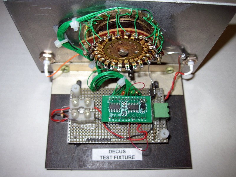
Photo 3 shows the front panel of the DECUS test fixture and Photo 4 shows the back of the DECUS test fixture.
Page 5
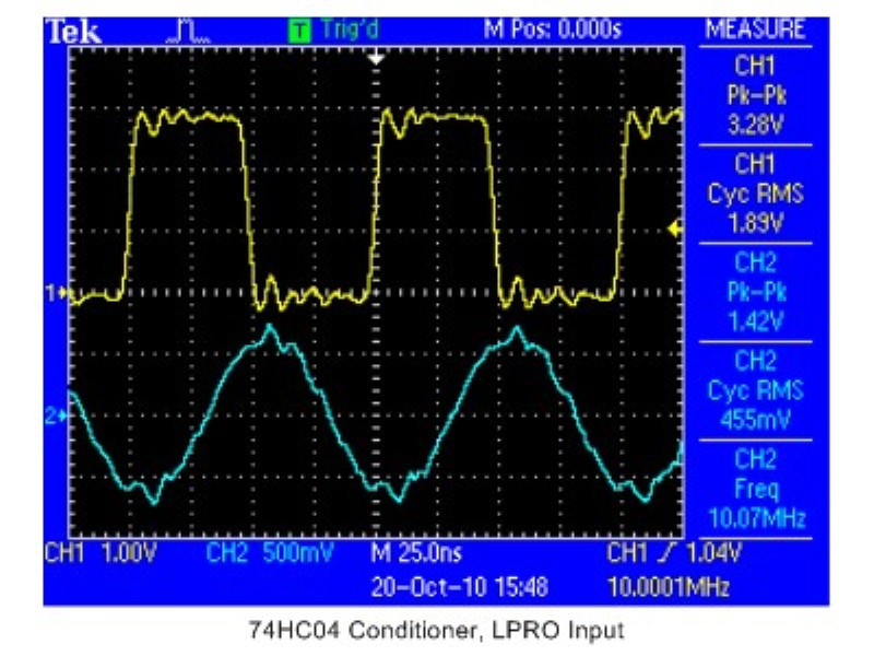
The input signal is applied between the module pins labeled "K" and "L" (ground), as shown in the schematic. The conditioning circuit is designed to be compatible with the LPRO-101 specifications with a typical input signal of 0.55 Volts RMS (approximately 1.5 Volts peak to peak). DECUS Photo 1 shows the typical input conditioning signals for a LPRO input.
Note: The input may not operate reliably for signal inputs under one Volt peak to peak. Inputs as high as 6 Volts peak to peak have been used but are not recommended for routine operation.
To verify the correct operation of the conditioning circuit, use an oscilloscope to observe the input signal between ground and pin 1 of the hex inverter. If the input voltage is within the range specified above, a 10 MHz square wave can be observed at pins "H", "T" and "V." Buffered versions of the conditioned signal appear at pins "J", "O" and "P" as shown in the schematic.
Page 6
The DECUS output frequencies and module pins are:
| C, F | 1 Megahertz |
| D, E | 100 Kilohertz |
| U, S | 25 Kilohertz |
| V, T, H | 10 Megahertz (unbuffered) |
| W | 10 Kilohertz |
| X | 1 Kilohertz |
| A | 100 Hertz |
| B | 1 Hertz |
| J, O, P | 10 Megahertz (buffered) |
I, Q |
Uncommmitted buffer outputs |
The above data and microprocessor port/pin mapping also appears on the schematic in the PIN/PORT MAPPING table.
Page 7
![]()
Power is applied to the DECUS module between pin "M" (positive) and pin "N" (ground). An alternate ground connection in at pin "L" of the module. Note that ground connections are also available on pads "X0-X3" but these are normally used only for testing -- they were part of an older jumper scheme and have been left on the PCB as test points.
An on-board 3.3 Volt regulator provides stable regulated power to the module.
Because each module is tested with an input voltage of 5 Volts, operation of the module is assured at this voltage. However, the specification sheet gives a typical (not maximum) dropout voltage of 1.7 volts and a worst-case minimum input voltage of 5.5 Volts. Thus, the input voltage should typically be 1.7 Volts above the output voltage. Although the nominal output voltage is 3.3 Volts we have seen outputs as low as 3.2 and as high as 3.4 Volts. If the regulator is replaced, the module power may need to be re-verified.
The module can operate from the 19 to 24 Volt rubidium oscillator supply if a 9.1 Volt zener diode is connected in series with the regulator's input.
The zener can be wired into the circuit by removing the shorting jumper across the zener on the bottom of the module (also see the schematic). When using the zener, the input voltage applied to the module should be a minimum of 15 Volts. For direct operation at lower voltages, such as 5 Volts, the shorting jumper should be left in place (the factory-wired default).
To use the zener diode, cut the shorting jumper across the diode on the bottom side of the board. The addition of the zener drops the regulator input voltage to approximately 15 Volts. Note that operating the module at higher input voltages (e.g., above 10 Volts) may significantly limit divider output currents, as noted below.
Once the proper input voltage has been selected, configured and applied to pin "M", the operation of the regulator can be verified by measuring the voltage betweeen ground and the power pins of the ICs. For example, 3.3 Volts should appear on pin 14 of the hex inverter and on pin 7 of the microprocessor. The measured voltage should be within a tenth of a Volt of 3.3 Volts. If the regulator is hot or the output voltage is not within specification, it is likely that the input voltage is too high or too low.
Page 8
Module quiescent current draw is approximately 12 milliamperes. For operation at higher input voltages, such as 24 Volts with a 9.1 Volt zener, total output buffering current may be limited to 5 milliamperes or less. Higher output currents are available when the module is operated at a lower input voltage (e.g., 5 Volts). If possible, operation with a lower supply voltage is recommended to reduce regulator stress and improve output current drive.
The maximum regulator dissipation is 250 milliwatts and the maximum regulator output current is 100 milliamperes. The regulator is both current and temperature limited in the event of output overload (e.g., due to higher input voltage or output loading).
Page 9
| Part | |||||
| R1,2 | RES 51.1K, 1/8W, 1%, 0805 | Digikey | 541-51.1KCCT-ND |
||
| R3 | RES, 1K, 1/8W, 1%, 0805 | Digikey | 541-1.00KCCT-ND |
||
| R4 | RES, 51R, 1/8W, 1%, 0805 | Digikey | 541-51.0CCT-ND |
||
| C1 | CAP, 100 pF, 200 Volt, NPO, 0805 | Digikey | PCC1977CT-ND |
||
| C2,5 | CAP, 10 uF, 6.3 Volt, X5R, 0805 | Digikey | PCC2225CT-ND |
||
| C3,4 | CAP, 1 uF, 25 Volt, X5R, 0805 | Digikey | PCC2319CT-ND |
||
| D1 | diode, zener, 1N4739, 9.1 Volt, 1 Watt, DO41 | Digikey | 1N4739ADICT-ND |
||
| D1 | REG, regulator, 3.3 Volt, TO-92, 100 mA, 250 mW | L78L33 |
|||
| IC1 | microprocessor, C8051T602-GS OTP, pre-programmed | Digikey | 336-1655-5-ND |
||
| IC2 | inverter, hex, 74LVC04ADR | Digikey | 296-1218-1-ND |
Page 10
| Part | |||||
| PCB1 | PCB, DECUS divider module | ||||
| PHD1,2 | 12-pin header, SIL, breakaway | FRYS | PLS-40S-P5 |
Page 11
Original circuit, board layout changes only |
||
Added R3, C4 to reset line - improved transient performance |
||
Replaced 74LVC04 with 74HC04 (less ringing) |
||
Reduced value of C1 to 100 pF |
||
Added 1N4739 to the board (now ships installed but shorted) |
||
Changed C3 and C2 to use stock parts |
||
Not implemented |
||
Added R4 and C5 to provide additional supply filtering for 74HC04, similar to that used in the LPRO manual. |
||
C3 and C2 can now be either 0805 or 1206 to use stock parts |
||
Changed so that there are now two uncommitted buffers with outputs at I and Q (no unused pins) |
||
Board is now shipped with R and G inputs connected to the 10 MHz output with short wire-wrap jumpers |
||
Board now has silk screen and solder mask. |